参数资料
| 型号: | ISL28133FEZ-T7 |
| 厂商: | Intersil |
| 文件页数: | 3/20页 |
| 文件大小: | 0K |
| 描述: | IC OPAMP CHOPPER RRIO SC70-5 |
| 产品培训模块: | Patient Monitoring and Diagnostic Equipment Solutions Solutions for Industrial Control Applications |
| 标准包装: | 3,000 |
| 放大器类型: | 断路器(零漂移) |
| 电路数: | 1 |
| 输出类型: | 满摆幅 |
| 转换速率: | 0.2 V/µs |
| 增益带宽积: | 400kHz |
| 电流 - 输入偏压: | 30pA |
| 电压 - 输入偏移: | 2µV |
| 电流 - 电源: | 18µA |
| 电流 - 输出 / 通道: | 26mA |
| 电压 - 电源,单路/双路(±): | 1.8 V ~ 5.5 V,±0.9 V ~ 2.75 V |
| 工作温度: | -40°C ~ 125°C |
| 安装类型: | 表面贴装 |
| 封装/外壳: | 6-TSSOP(5 引线),SC-88A,SOT-353 |
| 供应商设备封装: | SC-70-5 |
| 包装: | 带卷 (TR) |
ISL28133
11
FN6560.6
February 19, 2014
Applications Information
Functional Description
The ISL28133 uses a proprietary chopper-stabilized architecture
shown in the “Block Diagram” on page 2. The ISL28133
combines a 400kHz main amplifier with a very high open loop
gain (174dB) chopper stabilized amplifier to achieve very low
offset voltage and drift (2V, 0.02V/°C typical) while
consuming only 18A of supply current per channel.
This multi-path amplifier architecture contains a time continuous
main amplifier whose input DC offset is corrected by a
parallel-connected, high gain chopper stabilized DC correction
amplifier operating at 100kHz. From DC to ~5kHz, both
amplifiers are active with DC offset correction and most of the
low frequency gain is provided by the chopper amplifier. A 5kHz
crossover filter cuts off the low frequency amplifier path leaving
the main amplifier active out to the 400kHz gain-bandwidth
product of the device.
The key benefits of this architecture for precision applications are
very high open loop gain, very low DC offset, and low 1/f noise.
The noise is virtually flat across the frequency range from a few
mHz out to 100kHz, except for the narrow noise peak at the
amplifier crossover frequency (5kHz).
Rail-to-rail Input and Output (RRIO)
The RRIO CMOS amplifier uses parallel input PMOS and NMOS
that enable the inputs to swing 100mV beyond either supply rail.
The inverting and non-inverting inputs do not have back-to-back
input clamp diodes and are capable of maintaining high input
impedance at high differential input voltages. This is effective in
eliminating output distortion caused by high slew-rate input
signals.
The output stage uses common source connected PMOS and
NMOS devices to achieve rail-to-rail output drive capability with
17mA current limit and the capability to swing to within 20mV of
either rail while driving a 10k
Ω load.
IN+ and IN- Protection
All input terminals have internal ESD protection diodes to both
positive and negative supply rails, limiting the input voltage to
within one diode beyond the supply rails. For applications where
either input is expected to exceed the rails by 0.5V, an external
series resistor must be used to ensure the input currents never
exceed 20mA (see Figure 35).
Layout Guidelines for High Impedance Inputs
To achieve the maximum performance of the high input
impedance and low offset voltage of the ISL28133 amplifiers,
care should be taken in the circuit board layout. The PC board
surface must remain clean and free of moisture to avoid leakage
currents between adjacent traces. Surface coating of the circuit
board will reduce surface moisture and provide a humidity barrier,
reducing parasitic resistance on the board.
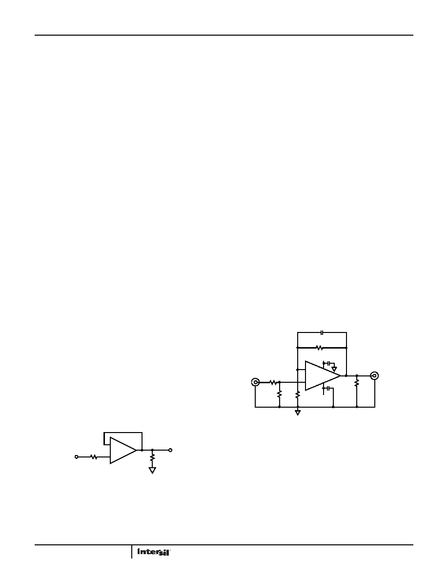
High Gain, Precision DC-Coupled Amplifier
The circuit in Figure 36 implements a single-stage, 10kV/V
DC-coupled amplifier with an input DC sensitivity of under 100nV
that is only possible using a low VOS amplifier with high open
loop gain. This circuit is practical down to 1.8V due to it's
rail-to-rail input and output capability. Standard high gain DC
amplifiers operating from low voltage supplies are not practical
at these high gains using typical low offset precision op amps
because the input offset voltage and temperature coefficient
consume most of the available output voltage swing. For
example, a typical precision amplifier in a gain of 10kV/V with a
±100V VOS and a temperature coefficient of 0.5V/°C would
produce a DC error at the output of >1V with an additional
5mV°C of temperature dependent error. At 3V, this DC error
consumes > 30% of the total supply voltage, making it
impractical to measure sub-microvolt low frequency signals.
The ±8V max VOS and 0.075V/°C of the ISL28133 produces a
temperature stable maximum DC output error of only ±80mV
with a maximum temperature drift of 0.75mV/°C. The additional
benefit of a very low 1/f noise corner frequency and some
feedback filtering enables DC voltages and voltage fluctuations
well below 100nV to be easily detected with a simple single
stage amplifier.
FIGURE 35. INPUT CURRENT LIMITING
-
+
RIN
RL
VIN
VOUT
FIGURE 36. HIGH GAIN, PRECISION DC-COUPLED AMPLIFIER
-
+
100
RL
VIN
VOUT
1M
100
-2.5V
+2.5V
ACL = 10kV/V
CF
0.018F
相关PDF资料 |
PDF描述 |
|---|---|
| 961242-6300-AR-PR | CONN HEADER STR DL 42PS GOLD SMD |
| MCP6S26T-I/ST | IC PGA 6CH R-R I/O 14TSSOP |
| ISL28117FUBZ-T7 | IC OPAMP GP 1.5MHZ LP 8MSOP |
| MCP6S26T-I/SL | IC PGA 6CH R-R I/O 14SOIC |
| 155208-5203-RB | CONN HEADER 2MM 8POS R/A .155" |
相关代理商/技术参数 |
参数描述 |
|---|---|
| ISL28133FEZ-T7A | 制造商:INTERSIL 制造商全称:Intersil Corporation 功能描述:Single, Dual, and Quad Micropower, Zero-Drift, RRIO Operational Amplifiers |
| ISL28133FHZ | 制造商:Intersil 功能描述:Single Micropower, Chopper Stabilized, RRIO Operational Amplifier |
| ISL28133FHZ-T7 | 功能描述:放大器 IC 开发工具 ISL28133FHZ MICROPWR PRCSN 5V CMOS OPER RoHS:否 制造商:International Rectifier 产品:Demonstration Boards 类型:Power Amplifiers 工具用于评估:IR4302 工作电源电压:13 V to 23 V |
| ISL28133FHZ-T7A | 功能描述:运算放大器 - 运放 ISL28133FHZ MICROPWR PRCSN 5V CMOS OPER RoHS:否 制造商:STMicroelectronics 通道数量:4 共模抑制比(最小值):63 dB 输入补偿电压:1 mV 输入偏流(最大值):10 pA 工作电源电压:2.7 V to 5.5 V 安装风格:SMD/SMT 封装 / 箱体:QFN-16 转换速度:0.89 V/us 关闭:No 输出电流:55 mA 最大工作温度:+ 125 C 封装:Reel |
| ISL28133FRUZ-T7 | 功能描述:放大器 IC 开发工具 ISL28133FRUZ SINGLE MIPR ZERO-DRIFT RoHS:否 制造商:International Rectifier 产品:Demonstration Boards 类型:Power Amplifiers 工具用于评估:IR4302 工作电源电压:13 V to 23 V |
发布紧急采购,3分钟左右您将得到回复。