- 您现在的位置:买卖IC网 > PDF目录383129 > ISL28138 (Intersil Corporation) 4.5MHz, Single and Dual Precision Rail-to-Rail Input-Output (RRIO) Op Amps with Very Low Input Bias Current(具有极低输入偏流的4.5MHz, 单/双精度轨对轨输入-输出(RRIO)运放) PDF资料下载
参数资料
| 型号: | ISL28138 |
| 厂商: | Intersil Corporation |
| 英文描述: | 4.5MHz, Single and Dual Precision Rail-to-Rail Input-Output (RRIO) Op Amps with Very Low Input Bias Current(具有极低输入偏流的4.5MHz, 单/双精度轨对轨输入-输出(RRIO)运放) |
| 中文描述: | 4.5MHz,单和双精密轨至轨输入,输出(RRIO)运算放大器,极低的输入偏置电流(具有极低输入偏流的4.5MHz,单/双精度轨对轨输入-输出(RRIO)运放) |
| 文件页数: | 12/16页 |
| 文件大小: | 861K |
| 代理商: | ISL28138 |
12
FN6336.1
June 28, 2007
Rail-to-Rail Output
A pair of complementary MOS devices are used to achieve
the rail-to-rail output swing. The NMOS sinks current to
swing the output in the negative direction. The PMOS
sources current to swing the output in the positive direction.
The ISL28138 and ISL28238 with a 100k
Ω
load will swing to
within 3mV of the positive supply rail and within 3mV of the
negative supply rail.
Results of Over-Driving the Output
Caution should be used when over-driving the output for long
periods of time. Over-driving the output can occur in two ways.
1) the input voltage times the gain of the amplifier exceeds the
supply voltage by a large value or 2) The output current
required is higher than the output stage can deliver. These
conditions can result in a shift in the Input Offset Voltage (V
OS
)
as much as 1μV/hr. of exposure under these condition.
IN+ and IN- Input Protection
All input terminals have internal ESD protection diodes to both
positive and negative supply rails, limiting the input voltage to
within one diode beyond the supply rails. They also contain
back-to-back diodes across the input terminals (Pin
Description Table - Circuit 1
)
. For applications where the input
differential voltage is expected to exceed 0.5V, an external
series resistor must be used to ensure the input currents
never exceed 5mA (Figure 42).
Enable/Disable Feature
The ISL28138 offers an EN pin that disables the device
when pulled up to at least 2.0V. In the disabled state (output
in a high impedance state), the part consumes typically 10μA
at room temperature. By disabling the part, multiple
ISL28138 parts can be connected together as a MUX. In this
configuration, the outputs are tied together in parallel and a
channel can be selected by the EN pin. The loading effects
of the feedback resistors of the disabled amplifier must be
considered when multiple amplifier outputs are connected
together. Note that feed through from the IN+ to IN- pins
occurs on any Mux Amp disabled channel where the input
differential voltage exceeds 0.5V (e.g., active channel
V
OUT
= 1V, while disabled channel V
IN
= GND), so the mux
implementation is best suited for small signal applications. If
large signals are required, use series IN+ resistors, or large
value R
F
, to keep the feed through current low enough to
minimize the impact on the active channel. See “Limitations
of the Differential Input Protection” on page 12 for more
details.The EN pin also has an internal pull-down. If left
open, the EN pin will pull to the negative rail and the device
will be enabled by default. When not used, the EN pin should
either be left floating or connected directly to the V- pin.
Limitations of the Differential Input Protection
If the input differential voltage is expected to exceed 0.5V, an
external current limiting resistor must be used to ensure the
input current never exceeds 5mA. For non-inverting unity gain
applications the current limiting can be via a series IN+ resistor,
or via a feedback resistor of appropriate value. For other gain
configurations, the series IN+ resistor is the best choice, unless
the feedback (R
F
) and gain setting (R
G
) resistors are both
sufficiently large to limit the input current to 5mA.
Large differential input voltages can arise from several
sources:
1) During open loop (comparator) operation. Used this way,
the IN+ and IN- voltages don’t track, so differentials arise.
2) When the amplifier is disabled but an input signal is still
present. An R
L
or R
G
to GND keeps the IN- at GND, while
the varying IN+ signal creates a differential voltage. Mux
Amp applications are similar, except that the active channel
V
OUT
determines the voltage on the IN- terminal.
3) When the slew rate of the input pulse is considerably
faster than the op amp’s slew rate. If the V
OUT
can’t keep up
with the IN+ signal, a differential voltage results, and visible
distortion occurs on the input and output signals. To avoid
this issue, keep the input slew rate below 4.8V/
μ
s, or use
appropriate current limiting resistors.
Large (>2V) differential input voltages can also cause an
increase in disabled I
CC
.
Using Only One Channel
If the application only requires one channel of the ISL28238
the user must configure the unused channel to prevent IT
from oscillating. The unused channel will oscillate if the input
and output pins are floating. This will result in higher than
expected supply currents and possible noise injection into
the channel being used. The proper way to prevent this
oscillation is to short the output to the negative input and
ground the positive input (as shown in Figure 43).
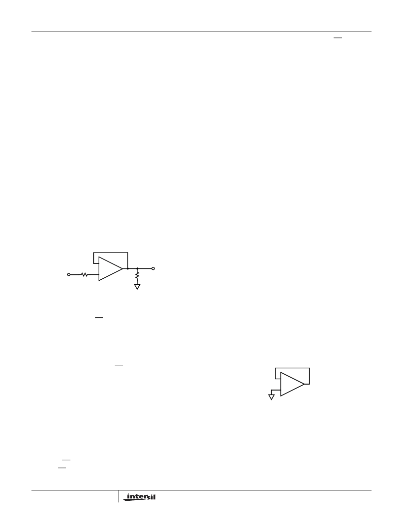
FIGURE 42. INPUT CURRENT LIMITING
-
+
R
IN
R
L
V
IN
V
OUT
FIGURE 43. PREVENTING OSCILLATIONS IN UNUSED
CHANNELS
-
+
ISL28138, ISL28238
相关PDF资料 |
PDF描述 |
|---|---|
| ISL28238 | 4.5MHz, Single and Dual Precision Rail-to-Rail Input-Output (RRIO) Op Amps with Very Low Input Bias Current(具有极低输入偏流的4.5MHz, 单/双精密轨对轨输入-输出(RRIO)运放) |
| ISL28158 | 34μA Micro-power Single and Dual Precision Rail-to-Rail Input-Output (RRIO) Low Input Bias Current Op Amps(34μA,微功率单/双精度轨对轨输入-输出(RRIO),低输入偏流运放) |
| ISL28258 | 34μA Micro-power Single and Dual Precision Rail-to-Rail Input-Output (RRIO) Low Input Bias Current Op Amps(34μA,微功率单/双精度轨对轨输入-输出(RRIO),低输入偏流运放) |
| ISL28476 | Dual and Quad Micropower Single Supply Rail-to-Rail Input and Output (RRIO) Precision Op Amp(双/四通道,微功率,单电源,轨对轨输入/输出(RRIO)精密运放) |
| ISL28276 | Dual and Quad Micropower Single Supply Rail-to-Rail Input and Output (RRIO) Precision Op Amp(双/四通道,微功率,单电源,轨对轨输入/输出(RRIO)精密运放) |
相关代理商/技术参数 |
参数描述 |
|---|---|
| ISL28138EVAL1Z | 功能描述:EVALUATION BOARD FOR ISL28138 RoHS:是 类别:编程器,开发系统 >> 评估板 - 运算放大器 系列:- 产品培训模块:Lead (SnPb) Finish for COTS Obsolescence Mitigation Program 标准包装:1 系列:- |
| ISL28138FBZ | 功能描述:IC OPAMP SGL/DUAL 4.5MHZ 8-SOIC RoHS:是 类别:集成电路 (IC) >> Linear - Amplifiers - Instrumentation 系列:- 其它有关文件:Automotive Product Guide 产品培训模块:Lead (SnPb) Finish for COTS Obsolescence Mitigation Program 标准包装:1 系列:- 放大器类型:通用 电路数:1 输出类型:满摆幅 转换速率:3 V/µs 增益带宽积:10MHz -3db带宽:- 电流 - 输入偏压:1pA 电压 - 输入偏移:70µV 电流 - 电源:2.5mA 电流 - 输出 / 通道:48mA 电压 - 电源,单路/双路(±):2.7 V ~ 5.5 V,±1.35 V ~ 2.75 V 工作温度:-40°C ~ 125°C 安装类型:表面贴装 封装/外壳:SOT-23-6 供应商设备封装:SOT-6 包装:Digi-Reel® 其它名称:MAX4475AUT#TG16DKR |
| ISL28138FBZ-T7 | 功能描述:IC OPAMP SGL/DUAL 4.5MHZ 8-SOIC RoHS:是 类别:集成电路 (IC) >> Linear - Amplifiers - Instrumentation 系列:- 其它有关文件:Automotive Product Guide 产品培训模块:Lead (SnPb) Finish for COTS Obsolescence Mitigation Program 标准包装:1 系列:- 放大器类型:通用 电路数:1 输出类型:满摆幅 转换速率:3 V/µs 增益带宽积:10MHz -3db带宽:- 电流 - 输入偏压:1pA 电压 - 输入偏移:70µV 电流 - 电源:2.5mA 电流 - 输出 / 通道:48mA 电压 - 电源,单路/双路(±):2.7 V ~ 5.5 V,±1.35 V ~ 2.75 V 工作温度:-40°C ~ 125°C 安装类型:表面贴装 封装/外壳:SOT-23-6 供应商设备封装:SOT-6 包装:Digi-Reel® 其它名称:MAX4475AUT#TG16DKR |
| ISL28138FHZ-T7 | 功能描述:IC OPAMP SGL/DUAL 4.5MHZ SOT23-6 RoHS:是 类别:集成电路 (IC) >> Linear - Amplifiers - Instrumentation 系列:- 其它有关文件:Automotive Product Guide 产品培训模块:Lead (SnPb) Finish for COTS Obsolescence Mitigation Program 标准包装:1 系列:- 放大器类型:通用 电路数:1 输出类型:满摆幅 转换速率:3 V/µs 增益带宽积:10MHz -3db带宽:- 电流 - 输入偏压:1pA 电压 - 输入偏移:70µV 电流 - 电源:2.5mA 电流 - 输出 / 通道:48mA 电压 - 电源,单路/双路(±):2.7 V ~ 5.5 V,±1.35 V ~ 2.75 V 工作温度:-40°C ~ 125°C 安装类型:表面贴装 封装/外壳:SOT-23-6 供应商设备封装:SOT-6 包装:Digi-Reel® 其它名称:MAX4475AUT#TG16DKR |
| ISL28138FHZ-T7A | 功能描述:IC OPAMP SGL RRIO 4.5MHZ SOT23-6 RoHS:是 类别:集成电路 (IC) >> Linear - Amplifiers - Instrumentation 系列:- 其它有关文件:Automotive Product Guide 产品培训模块:Lead (SnPb) Finish for COTS Obsolescence Mitigation Program 标准包装:1 系列:- 放大器类型:通用 电路数:1 输出类型:满摆幅 转换速率:3 V/µs 增益带宽积:10MHz -3db带宽:- 电流 - 输入偏压:1pA 电压 - 输入偏移:70µV 电流 - 电源:2.5mA 电流 - 输出 / 通道:48mA 电压 - 电源,单路/双路(±):2.7 V ~ 5.5 V,±1.35 V ~ 2.75 V 工作温度:-40°C ~ 125°C 安装类型:表面贴装 封装/外壳:SOT-23-6 供应商设备封装:SOT-6 包装:Digi-Reel® 其它名称:MAX4475AUT#TG16DKR |
发布紧急采购,3分钟左右您将得到回复。