- 您现在的位置:买卖IC网 > PDF目录16907 > ISL28166EVAL1Z (Intersil)EVALUATION BOARD FOR ISL28166 PDF资料下载
参数资料
| 型号: | ISL28166EVAL1Z |
| 厂商: | Intersil |
| 文件页数: | 2/11页 |
| 文件大小: | 0K |
| 描述: | EVALUATION BOARD FOR ISL28166 |
| 标准包装: | 1 |
| 每 IC 通道数: | 1 - 单 |
| 放大器类型: | 通用 |
| 输出类型: | 单端,满摆幅 |
| 转换速率: | 0.05 V/µs |
| 电流 - 输出 / 通道: | 31mA |
| 工作温度: | -40°C ~ 125°C |
| 电流供应(主 IC): | 39µA |
| 电压 - 电源,单路/双路(±): | 2.4 V ~ 5.5 V,±1.2 V ~ 2.75 V |
| 板类型: | 完全填充 |
| 已供物品: | 板 |
| 已用 IC / 零件: | ISL28166 |
10
All Intersil U.S. products are manufactured, assembled and tested utilizing ISO9001 quality systems.
Intersil Corporation’s quality certifications can be viewed at www.intersil.com/design/quality
Intersil products are sold by description only. Intersil Corporation reserves the right to make changes in circuit design, software and/or specifications at any time without
notice. Accordingly, the reader is cautioned to verify that data sheets are current before placing orders. Information furnished by Intersil is believed to be accurate and
reliable. However, no responsibility is assumed by Intersil or its subsidiaries for its use; nor for any infringements of patents or other rights of third parties which may result
from its use. No license is granted by implication or otherwise under any patent or patent rights of Intersil or its subsidiaries.
For information regarding Intersil Corporation and its products, see www.intersil.com
FN6155.5
January 16, 2014
Applications Information
Introduction
The ISL28166 is a BiMOS rail-to-rail input, output (RRIO)
operational amplifier with an enable feature. The device is
designed to operate from single supply (2.4V to 5.0V) or dual
supplies (±1.2V to ±2.5V) while drawing only 39A of supply
current. This combination of low power and precision
performance makes this device suitable for a variety of low
power applications including battery powered systems.
Rail-to-Rail Input/Output
This device feature bi-polar input which has an input
common mode range that extends to the rails and CMOS
outputs that can typically swing to within about 4mV of the
supply rails with a 100k
Ω load. The NMOS sinks current to
swing the output in the negative direction. The PMOS sources
current to swing the output in the positive direction.
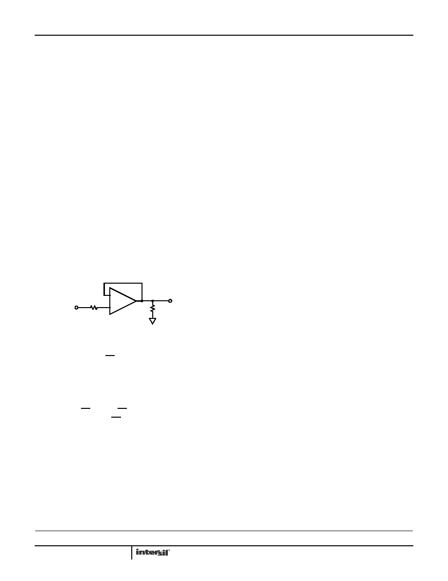
Input Protection
All input terminals have internal ESD protection diodes to both
positive and negative supply rails, limiting the input voltage to
within one diode beyond the supply rails. They also contain
back-to-back diodes across the input terminals. For
applications where the input differential voltage is expected to
exceed 0.5V, external series resistors must be used to ensure
the input currents never exceed 5mA (Figure 33).
Enable/Disable Feature
The ISL28166 offers an EN pin that disables the device
when pulled up to at least 2.0V. In the disabled state (output
in a high impedance state), the part consumes typically
10A. By disabling the part, multiple ISL28166 parts can be
connected together as a MUX. In this configuration, the
outputs are tied together in parallel and a channel can be
selected by the EN pin. The EN pin also has an internal
pull-down. If left open, the EN pin will pull to the negative rail
and the device will be enabled by default.
The loading effects of the feedback resistors of the disabled
amplifier must be considered when multiple amplifier outputs
are connected together.
Current Limiting
This device has no internal current-limiting circuitry. If the
output is shorted, it is possible to exceed the Absolute
Maximum Rating for output current or power dissipation,
potentially resulting in the destruction of the device.
Power Dissipation
It is possible to exceed the +125°C maximum junction
temperatures under certain load and power-supply
conditions. It is therefore important to calculate the
maximum junction temperature (TJMAX) for all applications
to determine if power supply voltages, load conditions, or
package type need to be modified to remain in the safe
operating area. These parameters are related in Equation 1:
where:
PDMAXTOTAL is the sum of the maximum power
dissipation of each amplifier in the package (PDMAX)
PDMAX for each amplifier can be calculated using
Equation 2:
where:
TMAX = Maximum ambient temperature
θJA = Thermal resistance of the package
PDMAX = Maximum power dissipation of 1 amplifier
VS = Supply voltage
IMAX = Maximum supply current of 1 amplifier
VOUTMAX = Maximum output voltage swing of the
application
RL = Load resistance
FIGURE 33. INPUT CURRENT LIMITING
-
+
RIN
RL
VIN
VOUT
T
JMAX
T
MAX
θ
JAxPDMAXTOTAL
()
+
=
(EQ. 1)
PD
MAX
2*V
S
I
SMAX
V
S
(
- V
OUTMAX )
V
OUTMAX
R
L
----------------------------
×
+
×
=
(EQ. 2)
ISL28166
相关PDF资料 |
PDF描述 |
|---|---|
| 202A142-25/225-0 | BOOT MOLDED |
| 342A112-25/86-0 | BOOT MOLDED |
| VI-JVM-EY | CONVERTER MOD DC/DC 10V 50W |
| VI-JVL-EY | CONVERTER MOD DC/DC 28V 50W |
| MIC2077-2BWM | IC USB DISTRIB SW QUAD 16-SOIC |
相关代理商/技术参数 |
参数描述 |
|---|---|
| ISL28166FHZ-T7 | 功能描述:IC OPAMP RRIO SGL 39UA SOT23-6 RoHS:是 类别:集成电路 (IC) >> Linear - Amplifiers - Instrumentation 系列:- 标准包装:1 系列:- 放大器类型:仪表 电路数:2 输出类型:满摆幅 转换速率:5 V/µs 增益带宽积:- -3db带宽:2MHz 电流 - 输入偏压:0.5pA 电压 - 输入偏移:250µV 电流 - 电源:415µA 电流 - 输出 / 通道:48mA 电压 - 电源,单路/双路(±):2.5 V ~ 5.5 V,±1.25 V ~ 2.75 V 工作温度:-55°C ~ 125°C 安装类型:表面贴装 封装/外壳:14-TSSOP(0.173",4.40mm 宽) 供应商设备封装:14-TSSOP 包装:剪切带 (CT) 产品目录页面:849 (CN2011-ZH PDF) 其它名称:296-12431-1296-12431-1-NDINA2331AIPWRCT |
| ISL28168 | 制造商:INTERSIL 制造商全称:Intersil Corporation 功能描述:34レA Micro-power Single and Dual Rail-to-Rail Input-Output (RRIO) Low Input Bias Current Op Amps |
| ISL28168_11 | 制造商:INTERSIL 制造商全称:Intersil Corporation 功能描述:Low Input Bias Current Op Amps |
| ISL28168EVAL1Z | 功能描述:EVALUATION BOARD FOR ISL28168 RoHS:是 类别:编程器,开发系统 >> 评估板 - 运算放大器 系列:- 产品培训模块:Lead (SnPb) Finish for COTS Obsolescence Mitigation Program 标准包装:1 系列:- |
| ISL28168FHZ-T7 | 功能描述:IC OPAMP RRIO SGL 34UA SOT23-6 RoHS:是 类别:集成电路 (IC) >> Linear - Amplifiers - Instrumentation 系列:- 其它有关文件:Automotive Product Guide 产品培训模块:Lead (SnPb) Finish for COTS Obsolescence Mitigation Program 标准包装:1 系列:- 放大器类型:通用 电路数:1 输出类型:满摆幅 转换速率:3 V/µs 增益带宽积:10MHz -3db带宽:- 电流 - 输入偏压:1pA 电压 - 输入偏移:70µV 电流 - 电源:2.5mA 电流 - 输出 / 通道:48mA 电压 - 电源,单路/双路(±):2.7 V ~ 5.5 V,±1.35 V ~ 2.75 V 工作温度:-40°C ~ 125°C 安装类型:表面贴装 封装/外壳:SOT-23-6 供应商设备封装:SOT-6 包装:Digi-Reel® 其它名称:MAX4475AUT#TG16DKR |
发布紧急采购,3分钟左右您将得到回复。