- 您现在的位置:买卖IC网 > PDF目录10763 > ISL28196FHZ-T7 (Intersil)IC COMPARATOR RRIO 2.5UA SOT23-6 PDF资料下载
参数资料
| 型号: | ISL28196FHZ-T7 |
| 厂商: | Intersil |
| 文件页数: | 3/14页 |
| 文件大小: | 0K |
| 描述: | IC COMPARATOR RRIO 2.5UA SOT23-6 |
| 标准包装: | 1 |
| 类型: | 通用 |
| 元件数: | 1 |
| 输出类型: | 推挽式,满摆幅 |
| 电压 - 电源,单路/双路(±): | 1.8 V ~ 5.5 V |
| 电压 - 输入偏移(最小值): | 2mV @ 5V |
| 电流 - 输入偏压(最小值): | 80pA @ 5V |
| 电流 - 静态(最大值): | 4µA |
| CMRR, PSRR(标准): | 100dB CMRR,100dB PSRR |
| 传输延迟(最大): | 300µs |
| 工作温度: | -40°C ~ 125°C |
| 封装/外壳: | SOT-23-6 |
| 安装类型: | 表面贴装 |
| 包装: | 标准包装 |
| 产品目录页面: | 1234 (CN2011-ZH PDF) |
| 其它名称: | ISL28196FHZ-T7DKR |
11
FN6152.4
September 29, 2008
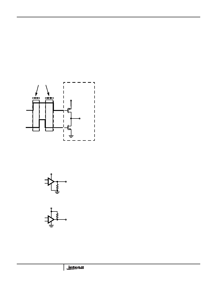
Break-Before-Make Operation of the Output
The output circuit has a break-before-make response. This
means that the P-Channel turns off before the N-Channel
turns on during a high to low transition of the output
(reference Figure 43). Likewise, the N-Channel turns off
before the P-Channel turns on during a low to high transition.
This results in different propagation delay times depending
upon where the output load resistor is tied to. If the load
resistor is tied to ground, (Figure 44A) then the propagation
delay is controlled by the P-Channel. For a high to low
transition the propagation delay does not include the
additional break-before-make time because the load resistor
will pull the output low once the P-Channel has turned off.
During the low to high transition, however, if the load resistor
is tied to ground, then the additional break-before-make time
is added to the propagation delay time because the output
won’t pull high until the P-Channel turns on.
If the load resistor is tied to V+ (Figure 44B) then the
propagation delay is controlled by the N-Channel. For this
condition, the additional delay time is added to the high to
low transition because the output won’t pull low until the
differences in propagation delay depending upon where the
load is tied.
Propagation Delay
The input to output propagation delay has a dependency on
power supply voltage, overdrive and whether the output is
decreasing time propagation delay vs supply voltage for the
ISL28196 and Figure 4 shows a similar behavior for the
ISL28197. The output break-before-make mechanism
results in a difference in propagation delay, depending on
whether the output stage NMOS and PMOS are sourcing or
sinking current. This delay difference is shown in the figures
as a function of where the load is terminated (+V or -V) and
also as a function of supply voltage. The dependence of
propagation delay as a function of power supply voltage and
Enable Feature
Both parts offer an EN pin, which enables the device when
pulled high. The enable threshold is referenced to the -V
terminal and has a level proportional to the total supply
Supply Voltage). The enable circuit has a delay time that
changes as a function of supply voltage. Figures 23 through
26 show the effect of supply voltage on the enable and
disable times. For supply voltages less than 3V, it is
recommended that the user account for the increase
enable/disable delay time.
In the disabled state (output in a high impedance state), the
supply current is reduced to a typical of only 2nA. By
disabling the devices, multiple parts can be connected
together as a MUX. In this configuration, the outputs are tied
together in parallel and a channel can be selected by the EN
pin. The EN pin should never be left floating. The EN pin
should be connnected directly to the V+ supply when not in
use.
Proper Layout Maximizes Performance
To achieve the maximum performance of the high input
impedance, care should be taken in the circuit board layout.
The PC board surface must remain clean and free of
moisture to avoid leakage currents between adjacent traces.
Surface coating of the circuit board will reduce surface
moisture and provide a humidity barrier, reducing parasitic
resistance on the board. When input leakage current is a
concern, the use of guard rings around the comparator
inputs will further reduce leakage currents.
FIGURE 44A. RL TO GND
FIGURE 44B. RL TO V+
FIGURE 44. CONNECTION OF RL TO GND AND V+
VOUT
v+
P-CHANNEL
N-CHANNEL
P-CH
O
N
P
-CH
OFF
N-CH
OFF
N-CH
ON
N-CH
OFF
P
-CH
ON
FIGURE 43. MAKE-BEFORE-BREAK ACTION OF THE
OUTPUT STAGE
ISL28196 AND ISL28197
OUTPUT STAGE
BREAK-BEFORE-MAKE
+
-
VOUT
V+
RL
+
-
VOUT
V+
RL
ISL28196, ISL28197
相关PDF资料 |
PDF描述 |
|---|---|
| VI-J24-MY-F4 | CONVERTER MOD DC/DC 48V 50W |
| VI-23X-CU-F2 | CONVERTER MOD DC/DC 5.2V 200W |
| VI-J24-MY-F3 | CONVERTER MOD DC/DC 48V 50W |
| VI-J24-MY-F2 | CONVERTER MOD DC/DC 48V 50W |
| VI-J23-MY-F4 | CONVERTER MOD DC/DC 24V 50W |
相关代理商/技术参数 |
参数描述 |
|---|---|
| ISL28196FRUZ-T7 | 功能描述:IC COMP RRIO SGL 2.5UA 6-TDFN RoHS:是 类别:集成电路 (IC) >> 线性 - 比较器 系列:- 产品培训模块:Lead (SnPb) Finish for COTS Obsolescence Mitigation Program 标准包装:2,500 系列:- 类型:通用 元件数:1 输出类型:CMOS,推挽式,满摆幅,TTL 电压 - 电源,单路/双路(±):2.5 V ~ 5.5 V,±1.25 V ~ 2.75 V 电压 - 输入偏移(最小值):5mV @ 5.5V 电流 - 输入偏压(最小值):1pA @ 5.5V 电流 - 输出(标准):- 电流 - 静态(最大值):24µA CMRR, PSRR(标准):80dB CMRR,80dB PSRR 传输延迟(最大):450ns 磁滞:±3mV 工作温度:-40°C ~ 85°C 封装/外壳:6-WFBGA,CSPBGA 安装类型:表面贴装 包装:管件 其它名称:Q3554586 |
| ISL28196FRUZ-TZ | 制造商:Intersil Corporation 功能描述: |
| ISL28197EVAL1Z | 功能描述:EVALUATION BOARD FOR ISL28197 RoHS:是 类别:编程器,开发系统 >> 评估演示板和套件 系列:- 产品培训模块:Obsolescence Mitigation Program 标准包装:1 系列:- 主要目的:电源管理,电池充电器 嵌入式:否 已用 IC / 零件:MAX8903A 主要属性:1 芯锂离子电池 次要属性:状态 LED 已供物品:板 |
| ISL28197FHZ-T7 | 功能描述:IC COMPARATOR RRIO 800NA SOT23-6 RoHS:是 类别:集成电路 (IC) >> 线性 - 比较器 系列:- 产品培训模块:Lead (SnPb) Finish for COTS Obsolescence Mitigation Program 标准包装:50 系列:- 类型:带电压基准 元件数:4 输出类型:开路漏极 电压 - 电源,单路/双路(±):2.5 V ~ 11 V,±1.25 V ~ 5.5 V 电压 - 输入偏移(最小值):10mV @ 5V 电流 - 输入偏压(最小值):- 电流 - 输出(标准):0.015mA @ 5V 电流 - 静态(最大值):8.5µA CMRR, PSRR(标准):80dB CMRR,80dB PSRR 传输延迟(最大):- 磁滞:- 工作温度:0°C ~ 70°C 封装/外壳:16-SOIC(0.154",3.90mm 宽) 安装类型:表面贴装 包装:管件 产品目录页面:1386 (CN2011-ZH PDF) |
| ISL28197FRUZ-T7 | 功能描述:IC COMP RRIO SGL 800NA 6-TDFN RoHS:是 类别:集成电路 (IC) >> 线性 - 比较器 系列:- 产品培训模块:Lead (SnPb) Finish for COTS Obsolescence Mitigation Program 标准包装:2,500 系列:- 类型:通用 元件数:1 输出类型:CMOS,推挽式,满摆幅,TTL 电压 - 电源,单路/双路(±):2.5 V ~ 5.5 V,±1.25 V ~ 2.75 V 电压 - 输入偏移(最小值):5mV @ 5.5V 电流 - 输入偏压(最小值):1pA @ 5.5V 电流 - 输出(标准):- 电流 - 静态(最大值):24µA CMRR, PSRR(标准):80dB CMRR,80dB PSRR 传输延迟(最大):450ns 磁滞:±3mV 工作温度:-40°C ~ 85°C 封装/外壳:6-WFBGA,CSPBGA 安装类型:表面贴装 包装:管件 其它名称:Q3554586 |
发布紧急采购,3分钟左右您将得到回复。