参数资料
| 型号: | ISL28214FBZ-T13 |
| 厂商: | Intersil |
| 文件页数: | 23/23页 |
| 文件大小: | 0K |
| 描述: | IC OPAMP GP RRIO 5MHZ DUAL 8SOIC |
| 标准包装: | 2,500 |
| 放大器类型: | 通用 |
| 电路数: | 2 |
| 输出类型: | 满摆幅 |
| 转换速率: | 2.5 V/µs |
| 增益带宽积: | 5MHz |
| 电流 - 输入偏压: | 3pA |
| 电压 - 输入偏移: | 500µV |
| 电流 - 电源: | 300µA |
| 电流 - 输出 / 通道: | 31mA |
| 电压 - 电源,单路/双路(±): | 1.8 V ~ 5.5 V,±0.9 V ~ 2.5 V |
| 工作温度: | -40°C ~ 125°C |
| 安装类型: | 表面贴装 |
| 封装/外壳: | 8-SOIC(0.154",3.90mm 宽) |
| 供应商设备封装: | 8-SOIC |
| 包装: | 带卷 (TR) |
ISL28114, ISL28214, ISL28414
9
FN6800.8
November 15, 2012
Applications Information
Functional Description
The ISL28114, ISL28214 and ISL28414 are single dual and
quad, CMOS rail-to-rail input, output (RRIO) micropower
operational amplifiers. They are designed to operate from single
supply (1.8V to 5.5V) or dual supply (±0.9V to ±2.75V). The parts
have an input common mode range that extends 100mV above
and below the power supply voltage rails. The output stage can
swing to within 15mV of the supply rails with a 10k load.
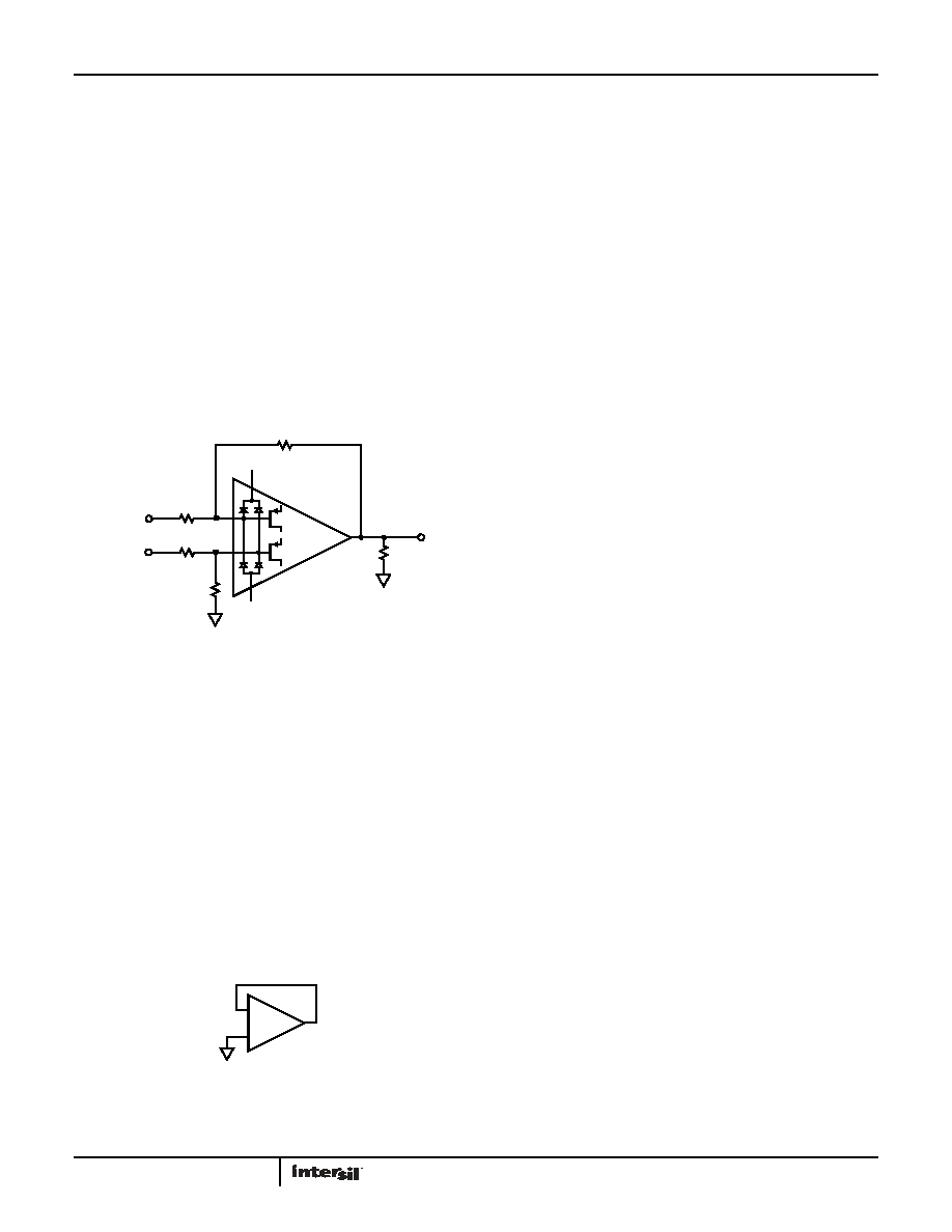
Input ESD Diode Protection
All input terminals have internal ESD protection diodes to both
positive and negative supply rails, limiting the input voltage to
within one diode beyond the supply rails. For applications where
the input differential voltage is expected to exceed 0.5V, an
external series resistor must be used to ensure the input currents
never exceed 20mA (see Figure 19).
Output Phase Reversal
Output phase reversal is a change of polarity in the amplifier
transfer function when the input voltage exceeds the supply
voltage. The ISL28114, ISL28214 and ISL28414 are immune to
output phase reversal, even when the input voltage is 1V beyond
the supplies.
Unused Channels
If the application requires less than all amplifiers one channel,
the user must configure the unused channel(s) to prevent it from
oscillating. The unused channel(s) will oscillate if the input and
output pins are floating. This will result in higher than expected
supply currents and possible noise injection into the channel
being used. The proper way to prevent this oscillation is to short
the output to the inverting input and ground the positive input (as
shown in Figure 20).
Power Dissipation
It is possible to exceed the +125°C maximum junction
temperatures under certain load, power supply conditions and
ambient temperature conditions. It is therefore important to
calculate the maximum junction temperature (TJMAX) for all
applications to determine if power supply voltages, load
conditions, or package type need to be modified to remain in the
safe operating area. These parameters are related using
Equation 1:
where:
PDMAXTOTAL is the sum of the maximum power dissipation of
each amplifier in the package (PDMAX)
where:
TMAX = Maximum ambient temperature
θJA = Thermal resistance of the package
PDMAX = Maximum power dissipation of 1 amplifier
VS = Total supply voltage
IqMAX = Maximum quiescent supply current of 1 amplifier
VOUTMAX = Maximum output voltage swing of the application
RL = Load resistance
ISL28114, ISL28214 and ISL28414 SPICE
Model
the net list for the SPICE model. The model is a simplified version
of the actual device and simulates important AC and DC
parameters. AC parameters incorporated into the model are: 1/f
and flatband noise, Slew Rate, CMRR, Gain and Phase. The DC
parameters are IOS, total supply current and output voltage swing.
The model uses typical parameters given in the “Electrical
Specifications” Table beginning on page 4. The AVOL is adjusted
for 90dB with the dominate pole at 125Hz. The CMRR is set 72dB,
f = 80kHz). The input stage models the actual device to present an
accurate AC representation. The model is configured for ambient
temperature of +25°C.
results for the Noise Voltage, Closed Loop Gain vs Frequency,
Large Signal 5V Step Response and CMRR and Open Loop Gain
Phase.
FIGURE 19. INPUT ESD DIODE CURRENT LIMITING
-
+
RIN-
RL
VIN-
V+
V-
RIN+
RF
RG
FIGURE 20. PREVENTING OSCILLATIONS IN UNUSED CHANNELS
-
+
TJMAX
TMAX θJAxPDMAXTOTAL
+
=
(EQ. 1)
PDMAX
VS IqMAX VS
(
- VOUTMAX)
VOUTMAX
RL
------------------------
×
+
×
=
(EQ. 2)
相关PDF资料 |
PDF描述 |
|---|---|
| 929647-03-36-EU | CONN HEADER 36POS STR .100" GOLD |
| 77313-162-28 | HDR STR DR .100 DP |
| 2534-5003UB | CONN HEADER 34POS R/A GOLD T/H |
| 77315-818-21 | CONN HEADER .100 1ROW R/A 21POS |
| 75844-102-16 | BERGSTIK STRAIGHT |
相关代理商/技术参数 |
参数描述 |
|---|---|
| ISL28214FBZ-T7 | 功能描述:IC OPAMP GP RRIO 5MHZ DUAL 8SOIC RoHS:是 类别:集成电路 (IC) >> Linear - Amplifiers - Instrumentation 系列:- 标准包装:2,500 系列:MicroAmplifier™ 放大器类型:通用 电路数:2 输出类型:- 转换速率:3.5 V/µs 增益带宽积:1MHz -3db带宽:- 电流 - 输入偏压:5pA 电压 - 输入偏移:1500µV 电流 - 电源:220µA 电流 - 输出 / 通道:60mA 电压 - 电源,单路/双路(±):4.5 V ~ 36 V,±2.25 V ~ 18 V 工作温度:-40°C ~ 85°C 安装类型:表面贴装 封装/外壳:8-SOIC(0.154",3.90mm 宽) 供应商设备封装:8-SOIC 包装:带卷 (TR) |
| ISL28214FHZ-T7 | 功能描述:运算放大器 - 运放 ISL28214FHZ Pb-Free Dual General Purpose Micropower, RRIO Op RoHS:否 制造商:STMicroelectronics 通道数量:4 共模抑制比(最小值):63 dB 输入补偿电压:1 mV 输入偏流(最大值):10 pA 工作电源电压:2.7 V to 5.5 V 安装风格:SMD/SMT 封装 / 箱体:QFN-16 转换速度:0.89 V/us 关闭:No 输出电流:55 mA 最大工作温度:+ 125 C 封装:Reel |
| ISL28214FHZ-T7A | 功能描述:运算放大器 - 运放 ISL28214FHZ Pb-Free Dual General Purpose Micropower, RRIO Op RoHS:否 制造商:STMicroelectronics 通道数量:4 共模抑制比(最小值):63 dB 输入补偿电压:1 mV 输入偏流(最大值):10 pA 工作电源电压:2.7 V to 5.5 V 安装风格:SMD/SMT 封装 / 箱体:QFN-16 转换速度:0.89 V/us 关闭:No 输出电流:55 mA 最大工作温度:+ 125 C 封装:Reel |
| ISL28214FUZ | 功能描述:IC OPAMP GP RRIO 5MHZ DUAL 8MSOP RoHS:是 类别:集成电路 (IC) >> Linear - Amplifiers - Instrumentation 系列:- 标准包装:73 系列:Over-The-Top® 放大器类型:通用 电路数:4 输出类型:满摆幅 转换速率:0.07 V/µs 增益带宽积:200kHz -3db带宽:- 电流 - 输入偏压:1nA 电压 - 输入偏移:285µV 电流 - 电源:50µA 电流 - 输出 / 通道:25mA 电压 - 电源,单路/双路(±):2 V ~ 44 V,±1 V ~ 22 V 工作温度:-40°C ~ 85°C 安装类型:表面贴装 封装/外壳:16-WFDFN 裸露焊盘 供应商设备封装:16-DFN-EP(5x3) 包装:管件 |
| ISL28214FUZ-T7 | 功能描述:IC OPAMP GP RRIO 5MHZ DUAL 8MSOP RoHS:是 类别:集成电路 (IC) >> Linear - Amplifiers - Instrumentation 系列:- 标准包装:2,500 系列:MicroAmplifier™ 放大器类型:通用 电路数:2 输出类型:- 转换速率:3.5 V/µs 增益带宽积:1MHz -3db带宽:- 电流 - 输入偏压:5pA 电压 - 输入偏移:1500µV 电流 - 电源:220µA 电流 - 输出 / 通道:60mA 电压 - 电源,单路/双路(±):4.5 V ~ 36 V,±2.25 V ~ 18 V 工作温度:-40°C ~ 85°C 安装类型:表面贴装 封装/外壳:8-SOIC(0.154",3.90mm 宽) 供应商设备封装:8-SOIC 包装:带卷 (TR) |
发布紧急采购,3分钟左右您将得到回复。