参数资料
| 型号: | ISL28227FUZ-T7 |
| 厂商: | Intersil |
| 文件页数: | 6/26页 |
| 文件大小: | 0K |
| 描述: | IC OPAMP PREC 10MHZ DL LN 8MSOP |
| 标准包装: | 1,500 |
| 放大器类型: | 通用 |
| 电路数: | 2 |
| 转换速率: | 3.6 V/µs |
| 增益带宽积: | 10MHz |
| 电流 - 输入偏压: | 1nA |
| 电压 - 输入偏移: | 10µV |
| 电流 - 电源: | 2.2mA |
| 电流 - 输出 / 通道: | 45mA |
| 电压 - 电源,单路/双路(±): | 4.5 V ~ 40 V,±2.25 V ~ 20 V |
| 工作温度: | -40°C ~ 125°C |
| 安装类型: | 表面贴装 |
| 封装/外壳: | 8-TSSOP,8-MSOP(0.118",3.00mm 宽) |
| 供应商设备封装: | 8-MSOP |
| 包装: | 带卷 (TR) |
ISL28127, ISL28227
14
FN6633.6
December 16, 2010
Applications Information
Functional Description
The ISL28127 and ISL28227 are single and dual, low noise
10MHz BW precision op amps. Both devices are fabricated in a
new precision 40V complementary bipolar DI process. A super-
beta NPN input stage with input bias current cancellation
provides low input bias current (1nA typical), low input offset
voltage (10V typ), low input noise voltage (3nV/
√Hz), and low
1/f noise corner frequency (5Hz). These amplifiers also feature
high open loop gain (1500V/mV) for excellent CMRR (120dB)
and THD+N performance (0.0002% @ 3.5VRMS, 1kHz into 2kΩ).
A complimentary bipolar output stage enables high capacitive
load drive without external compensation.
Operating Voltage Range
The devices are designed to operate over the 4.5V (±2.25V) to
40V (±20V) range and are fully characterized at 10V (±5V) and
30V (±15V). Parameter variation with operating voltage is shown
in the “Typical Performance Curves” beginning on page 8.
Input ESD Diode Protection
The input terminals (IN+ and IN-) have internal ESD protection
diodes to the positive and negative supply rails, and an additional
For unity gain applications (see Figure 38) where the output is
connected directly to the non-inverting input a current limiting
resistor (RIN) will be needed under the following conditions to
protect the anti-parallel differential input protection diodes.
The amplifier input is supplied from a low impedance source.
The input voltage rate-of-rise (dV/dt) exceeds the maximum
slew rate of the amplifier (±3.6V/s).
If the output lags far enough behind the input, the anti-parallel
input diodes can conduct. For example, if an input pulse ramps
from 0V to +10V in 1s, then the output of the ISL28x27 will reach
only +3.6V (slew rate = 3.6V/s) while the input is at 10V, The
input differential voltage of 6.4V will force input ESD diodes to
conduct, dumping the input current directly into the output stage
and the load. The resulting current flow can cause permanent
damage to the ESD diodes. The ESD diodes are rated to 20mA,
and in the previous example, setting RIN to 1k resistor (see Figure
38) would limit the current to < 6.4mA, and provide additional
protection up to ±20V at the input.
In applications where one or both amplifier input terminals are at
risk of exposure to high voltage, current limiting resistors may be
current through the power supply ESD diodes to 20mA.
Output Current Limiting
The output current is internally limited to approximately ±45mA
at +25°C and can withstand an short circuit to either rail as long
as the power dissipation limits are not exceeded. This applies to
only 1 amplifier at a time for the dual op amp. Continuous
operation under these conditions may degrade long term
reliability.
Output Phase Reversal
Output phase reversal is a change of polarity in the amplifier
transfer function when the input voltage exceeds the supply
voltage. The ISL28127 and ISL28227 are immune to output
phase reversal, even when the input voltage is 1V beyond the
supplies.
Power Dissipation
It is possible to exceed the +150°C maximum junction
temperatures under certain load and power supply conditions. It
is therefore important to calculate the maximum junction
temperature (TJMAX) for all applications to determine if power
supply voltages, load conditions, or package type need to be
modified to remain in the safe operating area. These parameters
are related using Equation 1:
where:
PDMAXTOTAL is the sum of the maximum power dissipation of
each amplifier in the package (PDMAX)
where:
TMAX = Maximum ambient temperature
θJA = Thermal resistance of the package
PDMAX = Maximum power dissipation of 1 amplifier
VS = Total supply voltage
IqMAX = Maximum quiescent supply current of 1 amplifier
VOUTMAX = Maximum output voltage swing of the application
RL = Load resistance
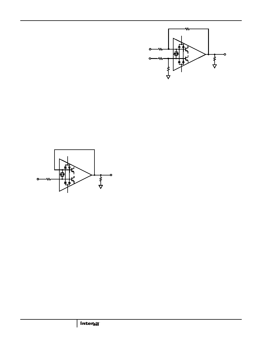
FIGURE 38. INPUT ESD DIODE CURRENT LIMITING- UNITY GAIN
-
+
RIN
RL
VIN
VOUT
V+
V-
FIGURE 39. INPUT ESD DIODE CURRENT LIMITING -
DIFFERENTIAL INPUT
-
+
RIN-
RL
VIN-
VOUT
V+
V-
RIN+
VIN+
TJMAX
TMAX θJAxPDMAXTOTAL
+
=
(EQ. 1)
PDMAX
VS IqMAX VS
(
- VOUTMAX)
VOUTMAX
RL
------------------------
×
+
×
=
(EQ. 2)
相关PDF资料 |
PDF描述 |
|---|---|
| 1544322-4 | CONN UNINS RECPT 17-20AWG 0.250 |
| CM1213-06MR | TVS ARRAY ESD PROT LOW 6CH 8MSOP |
| 208478096031049 | CONNECTOR RECEPT 96POS R/A |
| 77311-805-36LF | CONN HEADER 36POS VERT .100 15AU |
| ISL28118FBZ-T13 | IC OPAMP PREC R-R 4MHZ LP 8SOIC |
相关代理商/技术参数 |
参数描述 |
|---|---|
| ISL28227FUZ-T7A | 功能描述:精密放大器 ISL28227FUZ PREC LW NOISE OPERTNL AMP RoHS:否 制造商:Maxim Integrated 每芯片的通道数量: 输入补偿电压:0.25 mV at +/- 5 V 输入电压范围(最大值): 安装风格: 封装 / 箱体:SOIC-8 Narrow 封装:Tube |
| ISL28227SOICEVAL2Z | 功能描述:EVAL BOARD FOR ISL28227 SOIC RoHS:是 类别:编程器,开发系统 >> 评估板 - 运算放大器 系列:- 产品培训模块:Lead (SnPb) Finish for COTS Obsolescence Mitigation Program 标准包装:1 系列:- |
| ISL28230 | 制造商:INTERSIL 制造商全称:Intersil Corporation 功能描述:Single, Dual, and Quad Micropower, Low Drift, RRIO Operational Amplifiers |
| ISL28230CBZ | 功能描述:IC OPAMP GP RRIO 400KHZ DL 8SOIC RoHS:是 类别:集成电路 (IC) >> Linear - Amplifiers - Instrumentation 系列:- 其它有关文件:TS1854A View All Specifications 标准包装:50 系列:- 放大器类型:通用 电路数:4 输出类型:满摆幅 转换速率:0.25 V/µs 增益带宽积:630kHz -3db带宽:- 电流 - 输入偏压:16nA 电压 - 输入偏移:1000µV 电流 - 电源:162µA 电流 - 输出 / 通道:48mA 电压 - 电源,单路/双路(±):1.8 V ~ 6 V 工作温度:-40°C ~ 125°C 安装类型:表面贴装 封装/外壳:14-SOIC(0.154",3.90mm 宽) 供应商设备封装:14-SO 包装:管件 |
| ISL28230CBZ-T7 | 功能描述:IC OPAMP GP RRIO 400KHZ DL 8SOIC RoHS:是 类别:集成电路 (IC) >> Linear - Amplifiers - Instrumentation 系列:- 标准包装:1 系列:- 放大器类型:仪表 电路数:2 输出类型:满摆幅 转换速率:5 V/µs 增益带宽积:- -3db带宽:2MHz 电流 - 输入偏压:0.5pA 电压 - 输入偏移:250µV 电流 - 电源:415µA 电流 - 输出 / 通道:48mA 电压 - 电源,单路/双路(±):2.5 V ~ 5.5 V,±1.25 V ~ 2.75 V 工作温度:-55°C ~ 125°C 安装类型:表面贴装 封装/外壳:14-TSSOP(0.173",4.40mm 宽) 供应商设备封装:14-TSSOP 包装:剪切带 (CT) 产品目录页面:849 (CN2011-ZH PDF) 其它名称:296-12431-1296-12431-1-NDINA2331AIPWRCT |
发布紧急采购,3分钟左右您将得到回复。