- 您现在的位置:买卖IC网 > PDF目录16890 > ISL28246SOICEVAL1Z (Intersil)EVALUATION BOARD ISL28246 8SOIC PDF资料下载
参数资料
| 型号: | ISL28246SOICEVAL1Z |
| 厂商: | Intersil |
| 文件页数: | 3/16页 |
| 文件大小: | 0K |
| 描述: | EVALUATION BOARD ISL28246 8SOIC |
| 标准包装: | 1 |
| 每 IC 通道数: | 2 - 双 |
| 放大器类型: | 通用 |
| 输出类型: | 满摆幅 |
| 转换速率: | 1.9 V/µs |
| -3db带宽: | 13MHz |
| 电流 - 输出 / 通道: | 56mA |
| 工作温度: | -40°C ~ 125°C |
| 电流供应(主 IC): | 1mA |
| 电压 - 电源,单路/双路(±): | 2.4 V ~ 5.5 V,±1.2 V ~ 2.75 V |
| 板类型: | 完全填充 |
| 已供物品: | 板 |
| 已用 IC / 零件: | ISL28246 |
11
FN6321.3
June 23, 2008
Applications Information
Introduction
The ISL28146 and ISL28246 are single and dual channel
rail-to-rail input, output (RRIO) micropower precision
operational amplifiers. The parts are designed to operate
from single supply (2.4V to 5.0V) or dual supply (±1.2V to
±2.75V). The parts have an input common mode range that
extends 0.25V above the positive rail and down to the
negative supply rail. The output operation can swing within
about 3mV of the supply rails with a 100k
Ω load.
Rail-to-Rail Input
Many rail-to-rail input stages use two differential input pairs,
a long-tail PNP (or PFET) and an NPN (or NFET). Severe
penalties have to be paid for this circuit topology. As the
input signal moves from one supply rail to another, the
operational amplifier switches from one input pair to the
other causing drastic changes in input offset voltage and an
undesired change in magnitude and polarity of input offset
current.
The ISL28146 and ISL28246 achieve input rail-to-rail
operation without sacrificing important precision
specifications and degrading distortion performance. The
devices’ input offset voltage exhibits a smooth behavior
throughout the entire common-mode input range. The input
bias current versus the common-mode voltage range gives
an undistorted behavior from typically down to the negative
rail and up to 0.25V higher than the V+ rail.
Rail-to-Rail Output
A pair of complementary MOS devices are used to achieve
the rail-to-rail output swing. The NMOS sinks current to
swing the output in the negative direction. The PMOS
sources current to swing the output in the positive direction.
The ISL28146 and ISL28246 with a 100k
Ω load will swing to
within 3mV of the positive supply rail and within 3mV of the
negative supply rail.
Results of Over-Driving the Output
Caution should be used when over-driving the output for long
periods of time. Over-driving the output can occur in two ways:
1. The input voltage times the gain of the amplifier exceeds the
supply voltage by a large value.
2. The output current required is higher than the output stage
can deliver. These conditions can result in a shift in the Input
Offset Voltage (VOS) as much as 1V/hr. of exposure under
these conditions.
IN+ and IN- Input Protection
All input terminals have internal ESD protection diodes to both
positive and negative supply rails, limiting the input voltage to
within one diode beyond the supply rails. They also contain
back-to-back diodes across the input terminals (“Pin
the input differential voltage is expected to exceed 0.5V, an
external series resistor must be used to ensure the input
currents never exceed 5mA (Figure 36).
Enable/Disable Feature
The ISL28146 offers an EN pin that disables the device
when pulled up to at least 2.0V. In the disabled state (output
in a high impedance state), the part consumes typically 10A
at room temperature. The EN pin has an internal pull-down.
If left open, the EN pin will pull to the negative rail and the
device will be enabled by default. When not used, the EN pin
should either be left floating or connected directly to the -V
pin.
By disabling the part, multiple ISL28146 parts can be
connected together as a MUX. In this configuration, the
outputs are tied together in parallel and a channel can be
selected by the EN pin. The loading effects of the feedback
resistors of the disabled amplifier must be considered when
multiple amplifier outputs are connected together. Note that
feed through from the IN+ to IN- pins occurs on any Mux
Amp disabled channel where the input differential voltage
exceeds 0.5V (e.g., active channel VOUT = 1V, while
disabled channel VIN = GND), so the mux implementation is
best suited for small signal applications. If large signals are
required, use series IN+ resistors, or a large value RF, to
keep the feed through current low enough to minimize the
impact on the active channel. See “Limitations of the
Limitations of the Differential Input Protection
If the input differential voltage is expected to exceed 0.5V, an
external current limiting resistor must be used to ensure the
input current never exceeds 5mA. For non-inverting unity gain
applications, the current limiting can be via a series IN+ resistor,
or via a feedback resistor of appropriate value. For other gain
configurations, the series IN+ resistor is the best choice, unless
the feedback (RF) and gain setting (RG) resistors are both
sufficiently large to limit the input current to 5mA.
Large differential input voltages can arise from several
sources:
1. During open loop (comparator) operation. Used this way,
the IN+ and IN- voltages don’t track, so differentials arise.
2. When the amplifier is disabled but an input signal is still
present. An RL or RG to GND keeps the IN- at GND, while
the varying IN+ signal creates a differential voltage. Mux
Amp applications are similar, except that the active
channel VOUT determines the voltage on the IN- terminal.
3. When the slew rate of the input pulse is considerably
faster than the op amp’s slew rate. If the VOUT can’t keep
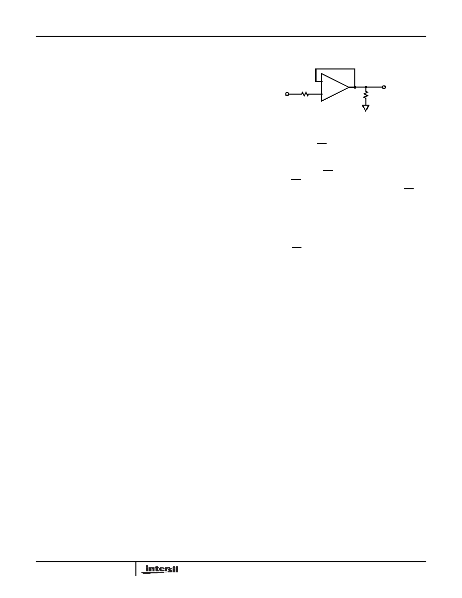
FIGURE 36. INPUT CURRENT LIMITING
-
+
RIN
RL
VIN
VOUT
ISL28146, ISL28246
相关PDF资料 |
PDF描述 |
|---|---|
| ISL28268MSOPEVAL1Z | EVALUATION BOARD ISL28268 8MSOP |
| FFMD-05-D-02.00-01 | CABLE ASSEM .05" 10POS M-M 2" |
| VI-23J-EY | CONVERTER MOD DC/DC 36V 50W |
| GBM25DREI | CONN EDGECARD 50POS .156 EYELET |
| HFA1110EVAL | EVALUATION PLATFORM HFA1110 |
相关代理商/技术参数 |
参数描述 |
|---|---|
| ISL28248 | 制造商:INTERSIL 制造商全称:Intersil Corporation 功能描述:4.5MHz, Single Dual and Quad Precision Rail-to-Rail Input-Output (RRIO) Op Amps with Very Low Input Bias Current |
| ISL28248FBZ | 功能描述:IC OP AMP DUAL RRIO 4.5MHZ 8SOIC RoHS:是 类别:集成电路 (IC) >> Linear - Amplifiers - Instrumentation 系列:- 标准包装:73 系列:Over-The-Top® 放大器类型:通用 电路数:4 输出类型:满摆幅 转换速率:0.07 V/µs 增益带宽积:200kHz -3db带宽:- 电流 - 输入偏压:1nA 电压 - 输入偏移:285µV 电流 - 电源:50µA 电流 - 输出 / 通道:25mA 电压 - 电源,单路/双路(±):2 V ~ 44 V,±1 V ~ 22 V 工作温度:-40°C ~ 85°C 安装类型:表面贴装 封装/外壳:16-WFDFN 裸露焊盘 供应商设备封装:16-DFN-EP(5x3) 包装:管件 |
| ISL28248FBZ-T7 | 功能描述:IC OP AMP DUAL RRIO 4.5MHZ 8SOIC RoHS:是 类别:集成电路 (IC) >> Linear - Amplifiers - Instrumentation 系列:- 标准包装:1 系列:- 放大器类型:仪表 电路数:2 输出类型:满摆幅 转换速率:5 V/µs 增益带宽积:- -3db带宽:2MHz 电流 - 输入偏压:0.5pA 电压 - 输入偏移:250µV 电流 - 电源:415µA 电流 - 输出 / 通道:48mA 电压 - 电源,单路/双路(±):2.5 V ~ 5.5 V,±1.25 V ~ 2.75 V 工作温度:-55°C ~ 125°C 安装类型:表面贴装 封装/外壳:14-TSSOP(0.173",4.40mm 宽) 供应商设备封装:14-TSSOP 包装:剪切带 (CT) 产品目录页面:849 (CN2011-ZH PDF) 其它名称:296-12431-1296-12431-1-NDINA2331AIPWRCT |
| ISL28248FUZ | 功能描述:IC OP AMP DUAL RRIO 4.5MHZ 8MSOP RoHS:是 类别:集成电路 (IC) >> Linear - Amplifiers - Instrumentation 系列:- 标准包装:73 系列:Over-The-Top® 放大器类型:通用 电路数:4 输出类型:满摆幅 转换速率:0.07 V/µs 增益带宽积:200kHz -3db带宽:- 电流 - 输入偏压:1nA 电压 - 输入偏移:285µV 电流 - 电源:50µA 电流 - 输出 / 通道:25mA 电压 - 电源,单路/双路(±):2 V ~ 44 V,±1 V ~ 22 V 工作温度:-40°C ~ 85°C 安装类型:表面贴装 封装/外壳:16-WFDFN 裸露焊盘 供应商设备封装:16-DFN-EP(5x3) 包装:管件 |
| ISL28248FUZ-T7 | 功能描述:IC OP AMP DUAL RRIO 4.5MHZ 8MSOP RoHS:是 类别:集成电路 (IC) >> Linear - Amplifiers - Instrumentation 系列:- 标准包装:1 系列:- 放大器类型:仪表 电路数:2 输出类型:满摆幅 转换速率:5 V/µs 增益带宽积:- -3db带宽:2MHz 电流 - 输入偏压:0.5pA 电压 - 输入偏移:250µV 电流 - 电源:415µA 电流 - 输出 / 通道:48mA 电压 - 电源,单路/双路(±):2.5 V ~ 5.5 V,±1.25 V ~ 2.75 V 工作温度:-55°C ~ 125°C 安装类型:表面贴装 封装/外壳:14-TSSOP(0.173",4.40mm 宽) 供应商设备封装:14-TSSOP 包装:剪切带 (CT) 产品目录页面:849 (CN2011-ZH PDF) 其它名称:296-12431-1296-12431-1-NDINA2331AIPWRCT |
发布紧急采购,3分钟左右您将得到回复。