参数资料
| 型号: | ISL28248FBZ-T7 |
| 厂商: | Intersil |
| 文件页数: | 5/18页 |
| 文件大小: | 0K |
| 描述: | IC OP AMP DUAL RRIO 4.5MHZ 8SOIC |
| 标准包装: | 1,000 |
| 放大器类型: | 通用 |
| 电路数: | 2 |
| 输出类型: | 满摆幅 |
| 转换速率: | 4 V/µs |
| 增益带宽积: | 4.5MHz |
| -3db带宽: | 13MHz |
| 电流 - 输入偏压: | 1pA |
| 电压 - 输入偏移: | 1800µV |
| 电流 - 电源: | 900µA |
| 电流 - 输出 / 通道: | 75mA |
| 电压 - 电源,单路/双路(±): | 2.4 V ~ 5.5 V,±1.2 V ~ 2.75 V |
| 工作温度: | -40°C ~ 125°C |
| 安装类型: | 表面贴装 |
| 封装/外壳: | 8-SOIC(0.154",3.90mm 宽) |
| 供应商设备封装: | 8-SOIC |
| 包装: | 带卷 (TR) |
13
FN6337.4
September 21, 2010
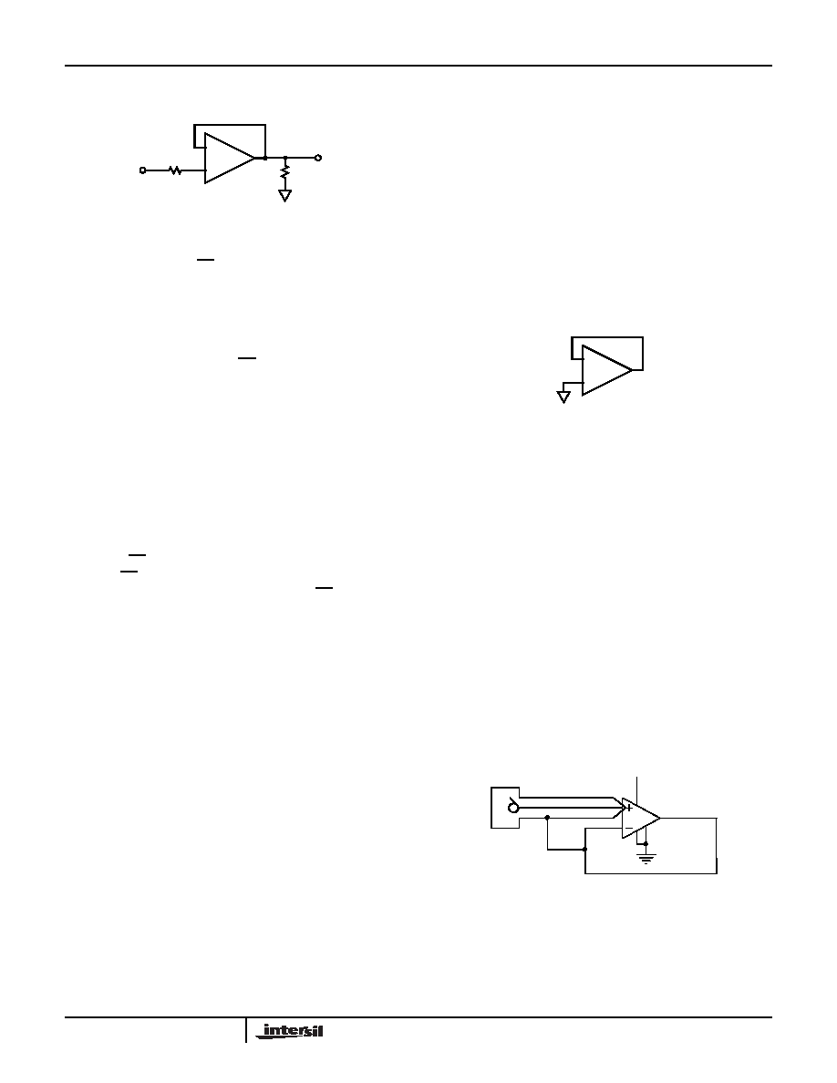
0.5V, an external series resistor must be used to ensure the
input currents never exceed 5mA (Figure 39).
Enable/Disable Feature
The ISL28148 offers an EN pin that disables the device
when pulled up to at least 2.0V. In the disabled state (output
in a high impedance state), the part consumes typically 10A
at room temperature. By disabling the part, multiple
ISL28148 parts can be connected together as a MUX. In this
configuration, the outputs are tied together in parallel and a
channel can be selected by the EN pin. The loading effects
of the feedback resistors of the disabled amplifier must be
considered when multiple amplifier outputs are connected
together. Note that feed-through from the IN+ to IN- pins
occurs on any Mux Amp disabled channel where the input
differential voltage exceeds 0.5V (e.g., active channel
VOUT = 1V, while disabled channel VIN = GND), so the mux
implementation is best suited for small signal applications. If
large signals are required, use series IN+ resistors, or large
value RF, to keep the feed-through current low enough to
minimize the impact on the active channel. See “Limitations
details.The EN pin also has an internal pull-down. If left
open, the EN pin will pull to the negative rail and the device
will be enabled by default. When not used, the EN pin should
either be left floating or connected directly to the V- pin.
Limitations of the Differential Input Protection
If the input differential voltage is expected to exceed 0.5V, an
external current limiting resistor must be used to ensure the
input current never exceeds 5mA. For non-inverting unity gain
applications the current limiting can be via a series IN+ resistor,
or via a feedback resistor of appropriate value. For other gain
configurations, the series IN+ resistor is the best choice, unless
the feedback (RF) and gain setting (RG) resistors are both
sufficiently large to limit the input current to 5mA.
Large differential input voltages can arise from several
sources:
During open loop (comparator) operation. Used this way,
the IN+ and IN- voltages don’t track, so differentials arise.
When the amplifier is disabled but an input signal is still
present. An RL or RG to GND keeps the IN- at GND, while
the varying IN+ signal creates a differential voltage. Mux
Amp applications are similar, except that the active
channel VOUT determines the voltage on the IN- terminal.
When the slew rate of the input pulse is considerably
faster than the op amp’s slew rate. If the VOUT can’t keep
up with the IN+ signal, a differential voltage results, and
visible distortion occurs on the input and output signals. To
avoid this issue, keep the input slew rate below 4.8V/s, or
use appropriate current limiting resistors.
Large (>2V) differential input voltages can also cause an
increase in disabled ICC.
Using Only One Channel
If the application does not use all channels, then the user
must configure the unused channel(s) to prevent them from
oscillating. The unused channel(s) will oscillate if the input
and output pins are floating. This will result in higher than
expected supply currents and possible noise injection into
the channel being used. The proper way to prevent this
oscillation is to short the output to the negative input and
ground the positive input (as shown in Figure 40).
Proper Layout Maximizes Performance
To achieve the maximum performance of the high input
impedance and low offset voltage, care should be taken in
the circuit board layout. The PC board surface must remain
clean and free of moisture to avoid leakage currents
between adjacent traces. Surface coating of the circuit board
will reduce surface moisture and provide a humidity barrier,
reducing parasitic resistance on the board. When input
leakage current is a concern, the use of guard rings around
the amplifier inputs will further reduce leakage currents.
Figure 41 shows a guard ring example for a unity gain
amplifier that uses the low impedance amplifier output at the
same voltage as the high impedance input to eliminate
surface leakage. The guard ring does not need to be a
specific width, but it should form a continuous loop around
both inputs. For further reduction of leakage currents,
components can be mounted to the PC board using Teflon
standoff insulators.
.
Current Limiting
These devices have no internal current-limiting circuitry. If
the output is shorted, it is possible to exceed the Absolute
Maximum Rating for output current or power dissipation,
potentially resulting in the destruction of the device.
FIGURE 39. INPUT CURRENT LIMITING
-
+
RIN
RL
VIN
VOUT
FIGURE 40. PREVENTING OSCILLATIONS IN UNUSED
CHANNELS
-
+
IN
V+
FIGURE 41. GUARD RING EXAMPLE FOR UNITY GAIN
AMPLIFIER
HIGH IMPEDANCE INPUT
ISL28148, ISL28248, ISL28448
相关PDF资料 |
PDF描述 |
|---|---|
| 68405-112HLF | BERGSTIK II DR R/A WIDE BODY |
| 108483012001025 | CONNECTOR HEADER 12POS STR |
| 521217-2 | TAB QUICK DISCONN 18-14AWG TIN |
| 10075025-G01-42ULF | CONN HEADER 42PS DL STR 2MM GOLD |
| M80-8270842 | CONN HDR 2MM SMT W/LATCH 8POS |
相关代理商/技术参数 |
参数描述 |
|---|---|
| ISL28248FUZ | 功能描述:IC OP AMP DUAL RRIO 4.5MHZ 8MSOP RoHS:是 类别:集成电路 (IC) >> Linear - Amplifiers - Instrumentation 系列:- 标准包装:73 系列:Over-The-Top® 放大器类型:通用 电路数:4 输出类型:满摆幅 转换速率:0.07 V/µs 增益带宽积:200kHz -3db带宽:- 电流 - 输入偏压:1nA 电压 - 输入偏移:285µV 电流 - 电源:50µA 电流 - 输出 / 通道:25mA 电压 - 电源,单路/双路(±):2 V ~ 44 V,±1 V ~ 22 V 工作温度:-40°C ~ 85°C 安装类型:表面贴装 封装/外壳:16-WFDFN 裸露焊盘 供应商设备封装:16-DFN-EP(5x3) 包装:管件 |
| ISL28248FUZ-T7 | 功能描述:IC OP AMP DUAL RRIO 4.5MHZ 8MSOP RoHS:是 类别:集成电路 (IC) >> Linear - Amplifiers - Instrumentation 系列:- 标准包装:1 系列:- 放大器类型:仪表 电路数:2 输出类型:满摆幅 转换速率:5 V/µs 增益带宽积:- -3db带宽:2MHz 电流 - 输入偏压:0.5pA 电压 - 输入偏移:250µV 电流 - 电源:415µA 电流 - 输出 / 通道:48mA 电压 - 电源,单路/双路(±):2.5 V ~ 5.5 V,±1.25 V ~ 2.75 V 工作温度:-55°C ~ 125°C 安装类型:表面贴装 封装/外壳:14-TSSOP(0.173",4.40mm 宽) 供应商设备封装:14-TSSOP 包装:剪切带 (CT) 产品目录页面:849 (CN2011-ZH PDF) 其它名称:296-12431-1296-12431-1-NDINA2331AIPWRCT |
| ISL28248MSOPEVAL1Z | 功能描述:EVAL BOARD FOR ISL28248 MSOP RoHS:是 类别:编程器,开发系统 >> 评估板 - 运算放大器 系列:- 产品培训模块:Lead (SnPb) Finish for COTS Obsolescence Mitigation Program 标准包装:1 系列:- |
| ISL28248SOICEVAL1Z | 功能描述:EVALUATION BOARD ISL28248 8SOIC RoHS:是 类别:编程器,开发系统 >> 评估板 - 运算放大器 系列:- 产品培训模块:Lead (SnPb) Finish for COTS Obsolescence Mitigation Program 标准包装:1 系列:- |
| ISL28256 | 制造商:INTERSIL 制造商全称:Intersil Corporation 功能描述:Low Input Bias Current Op Amps |
发布紧急采购,3分钟左右您将得到回复。