参数资料
| 型号: | ISL28273FAZ-T7 |
| 厂商: | Intersil |
| 文件页数: | 7/18页 |
| 文件大小: | 0K |
| 描述: | IC OPAMP DUAL RRIO MCPWR 16-QSOP |
| 产品培训模块: | Solutions for Industrial Control Applications |
| 标准包装: | 1 |
| 放大器类型: | 仪表 |
| 电路数: | 2 |
| 输出类型: | 满摆幅 |
| 转换速率: | 0.6 V/µs |
| -3db带宽: | 265kHz |
| 电流 - 输入偏压: | 1nA |
| 电压 - 输入偏移: | 12µV |
| 电流 - 电源: | 120µA |
| 电流 - 输出 / 通道: | 29mA |
| 电压 - 电源,单路/双路(±): | 2.5 V ~ 5.5 V,±1.25 V ~ 2.75 V |
| 工作温度: | -40°C ~ 125°C |
| 安装类型: | 表面贴装 |
| 封装/外壳: | 16-SSOP(0.154",3.90mm 宽) |
| 供应商设备封装: | 16-QSOP |
| 包装: | 标准包装 |
| 产品目录页面: | 1235 (CN2011-ZH PDF) |
| 其它名称: | ISL28273FAZ-T7DKR |
15
FN6260.6
October 21, 2009
range of input. See Input Bias Current vs Common-Mode
Input Voltage on page 8.
Input Bias Cancellation/Compensation
All three parts have an Input Bias Cancellation/Compensation
Circuit for both the input and feedback terminals (IN+, IN-, FB+
and FB-), achieving a low input bias current throughout the
input common-mode range and the operating temperature
range. While the PNP bipolar input stages are biased with an
adequate amount of biasing current for speed and increased
noise performance, the Input Bias Cancellation/Compensation
Circuit sinks most of the base current of the input transistors
leaving a small portion as input bias current, typically 500pA. In
addition, the Input Bias Cancellation/Compensation Circuit
maintains a smooth and flat behavior of input bias current over
the common mode range and over the operating temperature
range. The Input Bias Cancellation/Compensation Circuit
operates from input voltages of 10mV above the negative
supply to input voltages slightly above the positive supply. See
Input Bias Current vs Common-Mode Input Voltage in the
“Typical Performance Curves” on page 8.
Output Stage and Output Voltage Range
A Class AB common-source output stage drives the output.
The pair of complementary MOSFET devices drive the
output VOUT to within a few millivolts of the supply rails. At a
100k
Ω load, the PMOS sources current and pulls the output
up to 4mV below the positive supply. The NMOS sinks
current and pulls the output down to 4mV above the negative
supply, or ground in the case of a single supply operation.
The current sinking and sourcing capability are internally
limited to 29mA. When disabled, the outputs are in a high
impedance state.
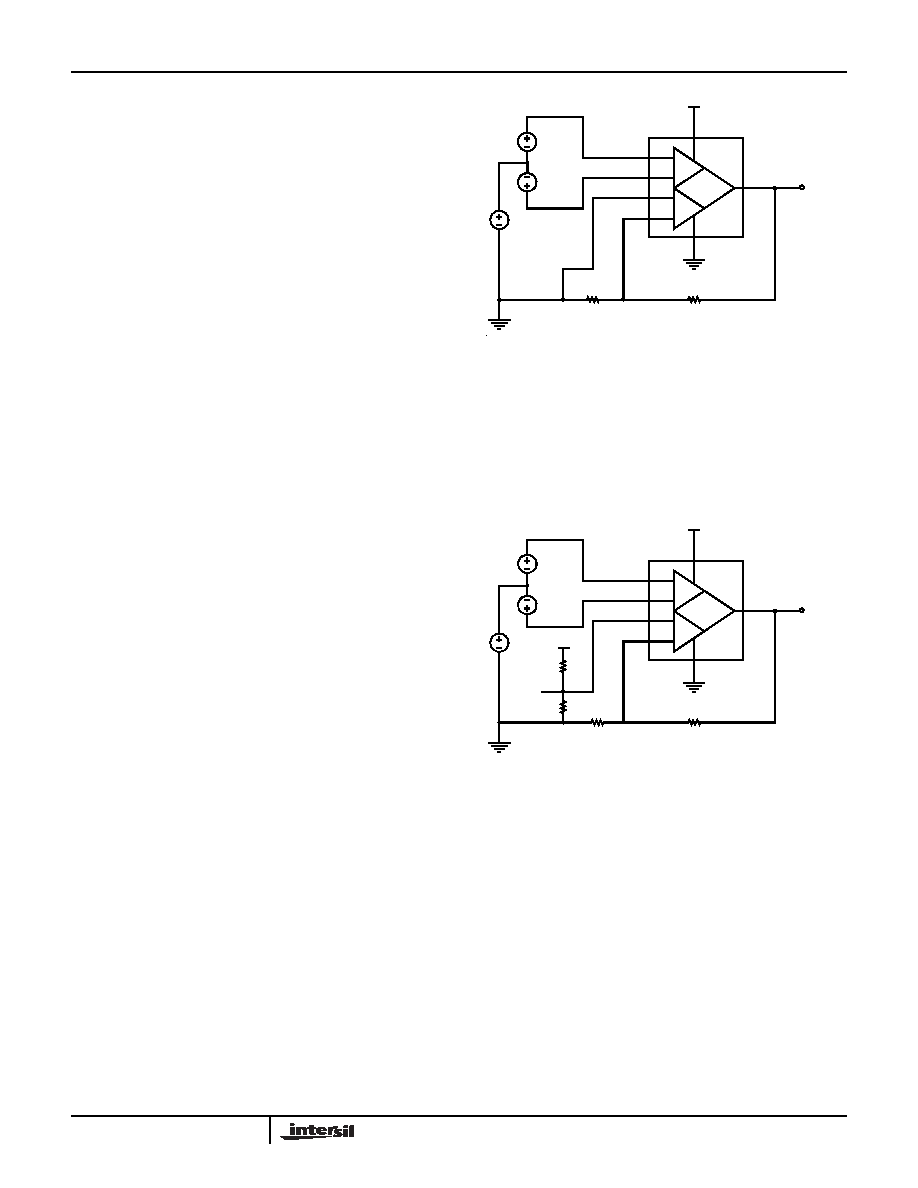
Gain Setting
VIN, the potential difference across IN+ and IN-, is replicated
(less the input offset voltage) across FB+ and FB-. The
function of the in-amp is to maintain the differential voltage
across FB- and FB+ equal to IN+ and IN-; (FB- - FB+) =
(IN+ - IN-). Consequently, the transfer function can be
derived. The in-amp gain is set by two external resistors, the
feedback resistor RF, and the gain resistor RG.
connected to GND. With this configuration, Equation 1 is
only true for a positive swing in VIN; negative input swings
will be ignored because the output will be at ground.
Reference Connection
Unlike a 3 op amp in-amp realization, a finite series
resistance seen at the REF terminal does not degrade the
high CMRR performance, eliminating the need for an
additional external buffer amplifier. Figure 50 uses the FB+
pin to provide a high impedance REF terminal.
The FB+ pin is used as a REF terminal to center or to adjust
the output. Because the FB+ pin is a high impedance input,
an economical resistor divider can be used to set the voltage
at the REF terminal without degrading or affecting the CMRR
performance. Any voltage applied to the REF terminal will
shift VOUT by VREF times the closed loop gain, which is set
by resistors RF and RG. Note that any noise or unwanted
signals on the reference supply will be amplified at the
The FB+ pin can also be connected to the other end of
VOUT
1
R
F
R
G
--------
+
VIN
=
VIN
IN+
IN-
–
=
(EQ. 1)
+
-
+
-
IN+
IN-
FB+
FB-
V+
V-
2.4V TO 5.5V
RF
RG
VOUT
VCM
IN+
IN-
FIGURE 49. GAIN IS SET BY TWO EXTERNAL RESISTORS,
RF AND RG
(ISL28270, ISL28470)
FIGURE 50. GAIN SETTING AND REFERENCE CONNECTION
+
-
+
-
IN+
IN-
FB+
FB-
V+
V-
2.4V TO 5.5V
RF
RG
VOUT
VCM
IN+
IN-
REF
2.9V to 5.5V
R1
R2
(ISL28270, ISL28470)
VIN
IN+
IN-
–
=
(EQ. 2)
VOUT
1
R
F
R
G
--------
+
VIN
()
1
R
F
R
G
--------
+
VREF
()
+
=
ISL28270, ISL28273, ISL28470
相关PDF资料 |
PDF描述 |
|---|---|
| MAX4492AUD+ | IC OPAMP QUAD R-R I/O 14-TSSOP |
| MAX4378TAUD+ | IC AMP CURRENT QUAD 14TSSOP |
| MAX4378FAUD+ | IC AMP CURRENT QUAD 14TSSOP |
| MAX4197ESA+ | IC AMP INSTRUMENT R-R 8-SOIC |
| MAX4195ESA+ | IC AMP INSTRUMENT R-R 8-SOIC |
相关代理商/技术参数 |
参数描述 |
|---|---|
| ISL28273INEVAL1Z | 功能描述:EVALUATION BOARD FOR ISL28273 RoHS:是 类别:编程器,开发系统 >> 评估板 - 运算放大器 系列:- 产品培训模块:Lead (SnPb) Finish for COTS Obsolescence Mitigation Program 标准包装:1 系列:- |
| ISL28274 | 制造商:INTERSIL 制造商全称:Intersil Corporation 功能描述:Micropower, Single Supply, Rail-to-Rail Input-Output Instrumentation Amplifier and Precision Operational Amplifier |
| ISL28274FAZ | 功能描述:IC INSTR/OP AMP RRIO SGL 16-QSOP RoHS:是 类别:集成电路 (IC) >> Linear - Amplifiers - Instrumentation 系列:- 标准包装:1 系列:- 放大器类型:通用 电路数:4 输出类型:满摆幅 转换速率:0.6 V/µs 增益带宽积:1MHz -3db带宽:- 电流 - 输入偏压:2pA 电压 - 输入偏移:1000µV 电流 - 电源:85µA 电流 - 输出 / 通道:20mA 电压 - 电源,单路/双路(±):1.8 V ~ 6 V 工作温度:-40°C ~ 125°C 安装类型:表面贴装 封装/外壳:14-SOIC(0.154",3.90mm 宽) 供应商设备封装:14-SOICN 包装:剪切带 (CT) 产品目录页面:680 (CN2011-ZH PDF) 其它名称:MCP6L04T-E/SLCT |
| ISL28274FAZ-T13 | 制造商:Intersil Corporation 功能描述: |
| ISL28274FAZ-T7 | 功能描述:IC INSTR/OP AMP RRIO SGL 16-QSOP RoHS:是 类别:集成电路 (IC) >> Linear - Amplifiers - Instrumentation 系列:- 其它有关文件:Automotive Product Guide 产品培训模块:Lead (SnPb) Finish for COTS Obsolescence Mitigation Program 标准包装:1 系列:- 放大器类型:通用 电路数:1 输出类型:满摆幅 转换速率:3 V/µs 增益带宽积:10MHz -3db带宽:- 电流 - 输入偏压:1pA 电压 - 输入偏移:70µV 电流 - 电源:2.5mA 电流 - 输出 / 通道:48mA 电压 - 电源,单路/双路(±):2.7 V ~ 5.5 V,±1.35 V ~ 2.75 V 工作温度:-40°C ~ 125°C 安装类型:表面贴装 封装/外壳:SOT-23-6 供应商设备封装:SOT-6 包装:Digi-Reel® 其它名称:MAX4475AUT#TG16DKR |
发布紧急采购,3分钟左右您将得到回复。