参数资料
| 型号: | ISL3036EIRZ-T |
| 厂商: | Intersil |
| 文件页数: | 16/16页 |
| 文件大小: | 0K |
| 描述: | IC LEVEL TRANSLATOR 4CH 14-TQFN |
| 标准包装: | 6,000 |
| 逻辑功能: | 变换器,双向 |
| 位数: | 4 |
| 输入类型: | 逻辑 |
| 输出类型: | 逻辑 |
| 数据速率: | 100Mbps |
| 通道数: | 4 |
| 输出/通道数目: | 1 |
| 差分 - 输入:输出: | 无/无 |
| 电源电压: | 2.2 V ~ 3.6 V |
| 工作温度: | -40°C ~ 85°C |
| 封装/外壳: | 14-VFDFN 裸露焊盘 |
| 供应商设备封装: | 14-QFN |
| 包装: | 带卷 (TR) |
9
FN6492.0
March 31, 2009
applications). The low static pull-up current is easily
overdriven by an active pull-down, and the feedback nature
of the accelerators (i.e., the accelerator firing in one direction
also triggers the accelerator in the opposite direction) aids
the passive pull-up once the input signal passes the
accelerator’s high threshold. The pull-up current and load
capacitance set the input signal rise time, and thus the
maximum data rate. For slow data rates the internal pull-up
current may suffice, but higher data rates - or more heavily
loaded signal lines - may require an external pull-up resistor.
Using External Bus Resistors
As mentioned earlier, these level translators incorporate I/O
pin pull-up current sources when enabled, and I/O pin
pull-up resistors in SHDN (except for the ISL3035E’s I/OVCC
pins). Therefore, external pull-up or pull-down resistors
shouldn’t be necessary, and aren’t recommended, unless
using high-speed open drain signaling.
Power Supplies
WIDE SUPPLY RANGE
These ICs operate from a wide range of supply voltages.
VL is designed to connect to the supply of 1.5V, 1.8V, and
2.5V powered devices, while VCC is targeted for 2.5V, and
3.3V components. Remember that VCC must be greater
than VL for proper operation.
POWER SUPPLY SEQUENCING
Either VCC or VL may be powered up first, but the IC
remains in SHDN until VCC exceeds VL by as much as
200mV. VL may exceed VCC by as much as 4V without
causing any damage.
I/O PIN INPUT THRESHOLDS VS SUPPLY VOLTAGE
Even though the “Electrical Specification” table on page 4
shows the I/O pin input thresholds (VIH, VIL) with a fixed
delta from the supplies or GND, the thresholds are better
represented as a percentage of the supplies. The typical
I/OVCC and CLK_VCC VIH runs about 55% to 60% of VCC,
while the corresponding VIL runs about 33% of VCC. The
typical I/OVL and CLK_VL VIH runs about 60% to 70% of VL,
while the corresponding VIL runs about 25% to 35% of VL.
Low Power SHDN Mode
This family of level translators features a low power SHDN
mode that tri-states all the I/O and output pins, considerably
reduces current consumption, and enables any pull-up
resistors on a port’s I/O pins (see Table 1). The ISL3034E
and ISL3036E enter the SHDN mode when the EN input
switches low, or automatically when the VCC voltage drops
below the VL voltage. The ISL3035 has no enable pin, so it
enters SHDN only if VCC drops below VL. The VL supply
powers the EN circuitry.
ISL3034E and ISL3036E
The ISL3034E and ISL3036E are general purpose level
translators featuring an enable pin, and six or four channels,
respectively. Both products include SHDN mode 16.5k
Ω
pull-ups on the I/OVCC and I/OVL pins.
ISL3035E
The ISL3035E specifically targets memory card applications,
and Figure 6 illustrates its use in an SD Card application.
Instead of six general purpose channels, the ISL3035E
features five general purpose channels and one dedicated
CLK channel. In memory card applications, the CLK channel
is a unidirectional signal driven by the host controller and
used by the memory card to synchronize data reads and
writes. The ISL3035E’s CLK channel is unique in that the
host CLK applied to the CLK_VL pin routes to the memory
card via the CLK_VCC pin, but it also loops back to the host
on the CLK_RET pin. This CLK_RET signal better mimics
the timing of “read” data returned from the memory card (see
Figure 21 for signal timing), so using CLK_RET as the host’s
input CLK improves the CLK to data timing relationship.
CLK_RET is strictly an output, and CLK_VL is strictly an
input. If an ISL3035E application needs a sixth I/O channel
then the user needs to connect CLK_VL and CLK_RET
together. Connected this way, the combination channel has the
same architecture as the other I/O channels. Both CLK_RET
and CLK_VL have equivalent pull-up current sources and
SHDN pull-up resistors, so connecting these two pins together
doubles the pull-up current in either mode.
The bit-by-bit auto direction control eliminates the need for
GPIO signals to control the flow of data on the CMD and
DAT lines.
The ISL3035E has no enable pin, so it only enters the low
power SHDN mode when VCC drops below VL. There are no
SHDN pull-up resistors on the I/OVCC and CLK_VCC pins,
but there are 75k
Ω pull-ups on the I/OV
L, CLK_VL, and
CLK_RET pins.
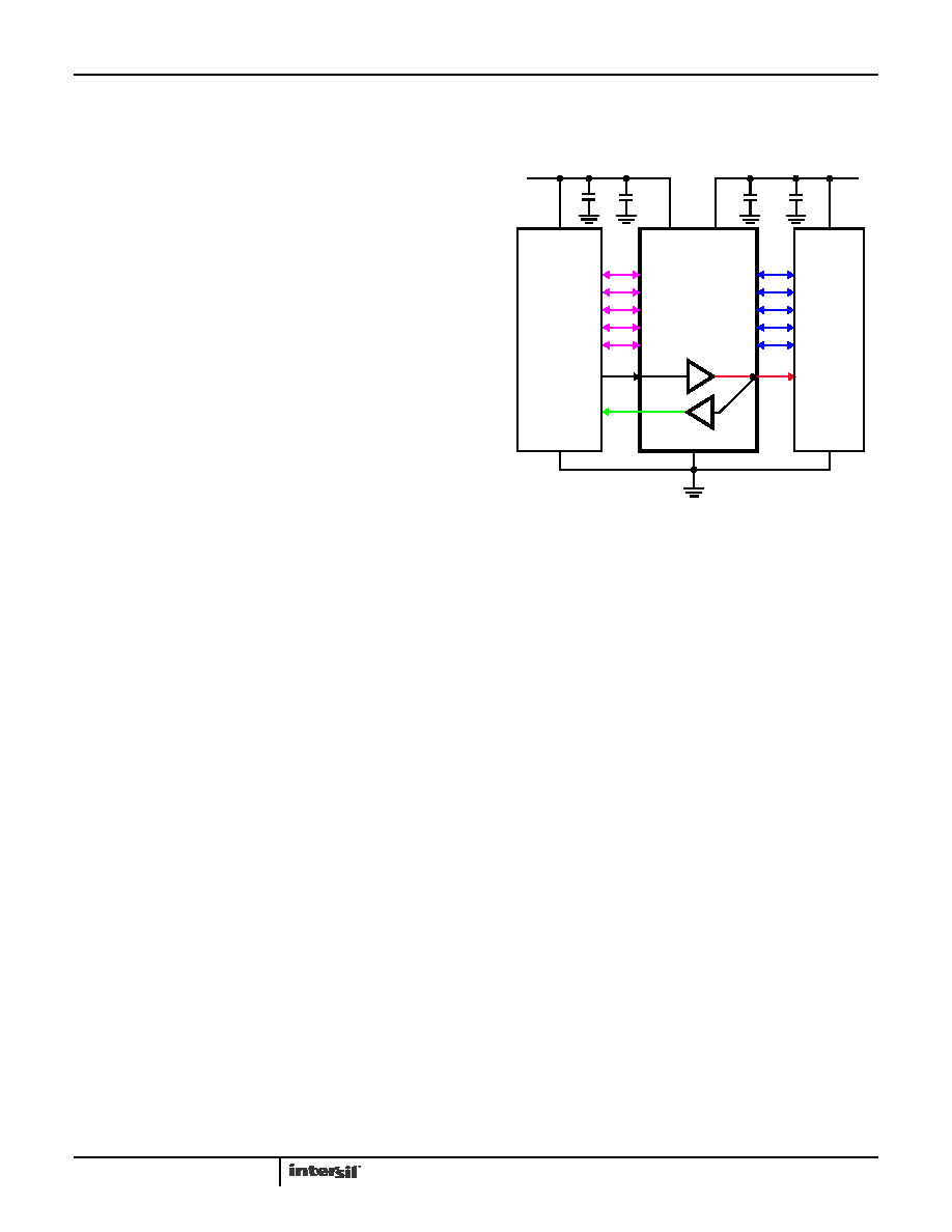
FIGURE 6. ISL3035E IN AN SD CARD APPLICATION
VL
VCC
I/OVL_
ISL3035E
CLK_RET
I/OVL_
GND
I/OVCC_
CLK_VL
CLK_VCC
DAT3
DAT2
DAT1
DAT0
CMD
CLOCK
GND
+3.3V
SD CARD
DAT3
DAT2
CLOCK_IN
DAT1
DAT0
CMD
CLOCK
+1.8V
SYSTEM
CONTROLLER
0.1
F
0.1
F
+1.8V
1
F
+3.3V
HOST
1
F
ISL3034E, ISL3035E, ISL3036E
相关PDF资料 |
PDF描述 |
|---|---|
| ISL3035EIRUZ-T | IC LEVEL TRANSLATOR 6CH 16TQFN |
| ICS552ARI-01 | IC OSC/MULT/BUFFER OCT 20-SSOP |
| MS27468T13B8BA | CONN HSG RCPT 8POS JAMNUT SCKT |
| MS3124F24-61S | CONN RCPT 61POS JAM NUT W/SCKT |
| MS27474T22B32PLC | CONN HSG RCPT 32POS JAM NUT PINS |
相关代理商/技术参数 |
参数描述 |
|---|---|
| ISL3036EIRZ-T7A | 功能描述:转换 - 电压电平 QD LVL SHIFTER ESD 1 4LD 3 5X3 5MM IND W RoHS:否 制造商:Micrel 类型:CML/LVDS/LVPECL to LVCMOS/LVTTL 传播延迟时间:1.9 ns 电源电流:14 mA 电源电压-最大:3.6 V 电源电压-最小:3 V 最大工作温度:+ 85 C 安装风格:SMD/SMT 封装 / 箱体:MLF-8 |
| ISL3036EIRZ-TK | 功能描述:IC LEVEL TRANSLATOR 4CH 14-TQFN RoHS:是 类别:集成电路 (IC) >> 逻辑 - 变换器 系列:- 产品培训模块:Lead (SnPb) Finish for COTS Obsolescence Mitigation Program 标准包装:100 系列:- 逻辑功能:变换器,双向 位数:2 输入类型:CMOS 输出类型:CMOS 数据速率:16Mbps 通道数:2 输出/通道数目:1 差分 - 输入:输出:无/无 传输延迟(最大):15ns 电源电压:1.65 V ~ 5.5 V 工作温度:-40°C ~ 85°C 封装/外壳:10-UFQFN 供应商设备封装:10-UTQFN(1.4x1.8) 包装:管件 |
| ISL3084 | 制造商:INTERSIL 制造商全称:Intersil Corporation 功能描述:5GHz VCO |
| ISL3084IR | 制造商:INTERSIL 制造商全称:Intersil Corporation 功能描述:5GHz VCO |
| ISL3084IR-TK | 制造商:INTERSIL 制造商全称:Intersil Corporation 功能描述:5GHz VCO |
发布紧急采购,3分钟左右您将得到回复。