- 您现在的位置:买卖IC网 > PDF目录16320 > ISL34341KIT1Z (Intersil)EVAL KIT FOR ISL34341 PDF资料下载
参数资料
| 型号: | ISL34341KIT1Z |
| 厂商: | Intersil |
| 文件页数: | 5/11页 |
| 文件大小: | 0K |
| 描述: | EVAL KIT FOR ISL34341 |
| 产品培训模块: | Solutions for Industrial Control Applications |
| 标准包装: | 1 |
| 系列: | * |
3
FN6827.1
October 8, 2010
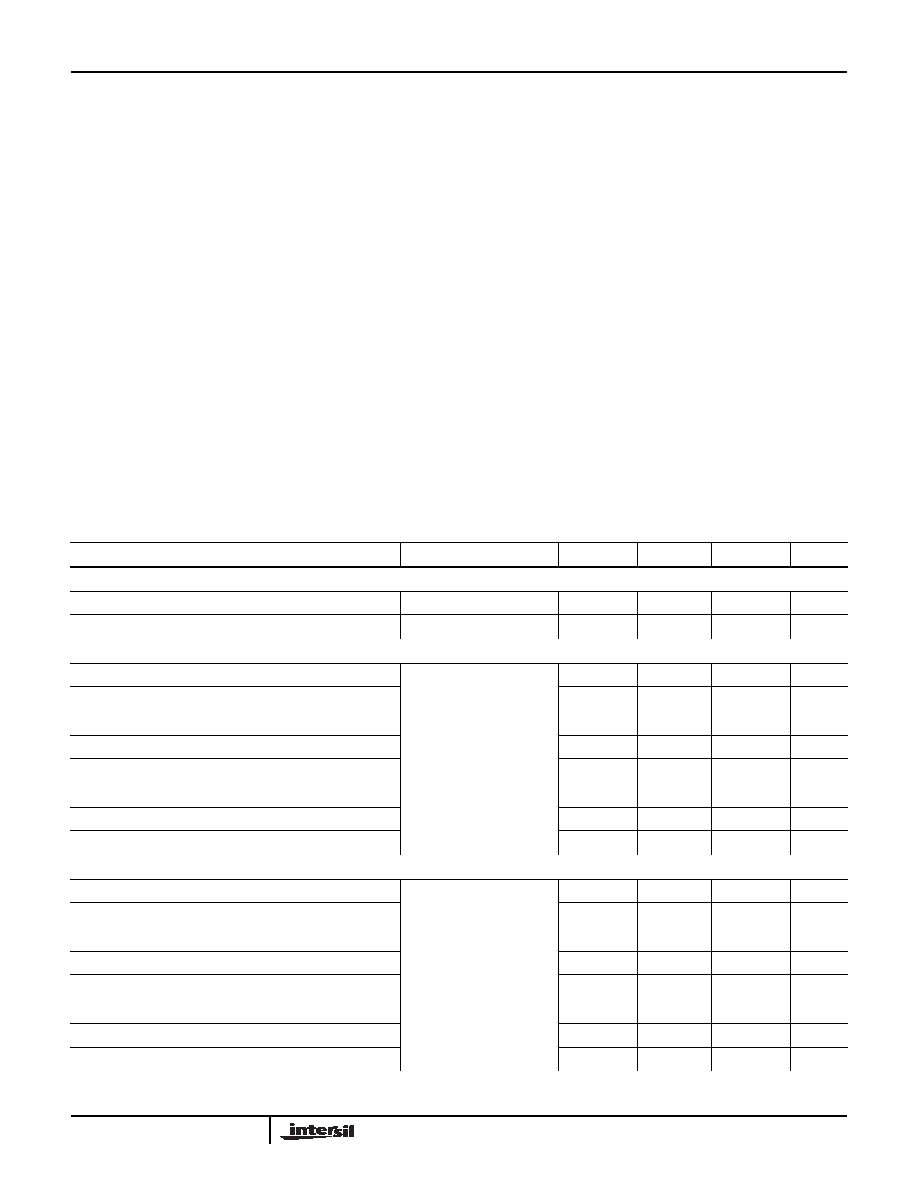
Absolute Maximum Ratings
Thermal Information
Supply Voltage
VDD_P to GND_P, VDD_TX to GND_TX,
VDD_IO to GND_IO . . . . . . . . . . . . . . . . . . . . . . . -0.5V to 4.6V
VDD_CDR to GND_CDR, VDD_CR to GND_CR . . -0.5V to 2.5V
Between any pair of GND_P, GND_TX,
GND_IO, GND_CDR, GND_CR . . . . . . . . . . . . . -0.1V to 0.1V
3.3V Tolerant LVTTL/LVCMOS
Input Voltage . . . . . . . . . . . . . . . . . . . . . .-0.3V to VDD_IO + 0.3V
Differential Input Voltage . . . . . . . . . . . . . . .-0.3V to VDD_IO + 0.3V
Differential Output Current . . . . . . . . . . . . . .Short Circuit Protected
LVTTL/LVCMOS Outputs . . . . . . . . . . . . . . . .Short Circuit Protected
ESD Rating
Human Body Model
All pins . . . . . . . . . . . . . . . . . . . . . . . . . . . . . . . . . . . . . . . . .4kV
SERIOP/N (all VDD Connected, all GND Connected) . . . . .8kV
Machine Model . . . . . . . . . . . . . . . . . . . . . . . . . . . . . . . . . . . .200V
Thermal Resistance (Typical, Notes 1, 2)
θJA
θJC (°C/W)
EPTQFP. . . . . . . . . . . . . . . . . . . . . . . .
40
12
Maximum Power Dissipation. . . . . . . . . . . . . . . . . . . . . . . . . . . . 327mW
Maximum Junction Temperature . . . . . . . . . . . . . . . . . . . . . . +125°C
Maximum Storage Temperature Range . . . . . . . . . .-65°C to +150°C
Operating Temperature Range . . . . . . . . . . . . . . . . .-40°C to +85°C
Pb-Free Reflow Profile. . . . . . . . . . . . . . . . . . . . . . . . .see link below
CAUTION: Do not operate at or near the maximum ratings listed for extended periods of time. Exposure to such conditions may adversely impact product reliability and
result in failures not covered by warranty.
NOTES:
1.
θJA is measured in free air with the component mounted on a high effective thermal conductivity test board with “direct attach” features. See
Tech Brief TB379.
2. For
θJC, the “case temp” location is the center of the exposed metal pad on the package underside.
Electrical Specifications
Unless otherwise indicated, all data is for: VDD_CDR = VDD_CR = 1.8V, VDD_IO = 3.3V,
VDD_TX = VDD_P = VDD_AN = 3.3V, TA = +25°C, Ref_Res = 3.16kΩ, High-speed AC-coupling
capacitor = 27nF.
PARAMETER
SYMBOL
CONDITIONS
MIN
TYP
MAX
UNITS
POWER SUPPLY VOLTAGE
VDD_CDR, VDD_CR
1.7
1.8
1.9
V
VDD_TX, VDD_P, VDD_AN, VDD_IO
3.0
3.3
3.6
V
SERIALIZER POWER SUPPLY CURRENTS
Analog TX Supply Current
IDDTX
VIDEO_TX = 1
PCLK_IN = 40MHz
17
mA
Analog CDR Supply Current
IDDCDR
57
mA
Digital I/O Supply Current
IDDIO
12
mA
Digital Supply Current
IDDCR
20
mA
PLL/VCO Supply Current
IDDP
17
mA
Analog Bias Supply Current
IDDAN
5.5
mA
Total 1.8V Supply Current
77
90
mA
Total 3.3V Supply Current
40
46
mA
DESERIALIZER POWER SUPPLY CURRENTS
Analog TX Supply Current
IDDTX
VIDEO_TX = 0
REF_CLK = 40MHz
24
mA
Analog CDR Supply Current
IDDCDR
45
mA
Digital I/O Supply Current
IDDIO
17
25
mA
Digital Supply Current
IDDCR
32
mA
PLL/VCO Supply Current
IDDP
17
mA
Analog Bias Supply Current
IDDAN
5.4
mA
Total 1.8V Supply Current
77
90
mA
Total 3.3V Supply Current
64
80
mA
ISL34341
相关PDF资料 |
PDF描述 |
|---|---|
| VI-J1T-EZ-F1 | CONVERTER MINIMOD DC/DC 6.5V 25W |
| ISL59605-SPI-EVALZ | EVAL BOARD FOR ISL5960X |
| ADM691AANZ | IC SUPERVISOR MPU 4.65V 16DIP |
| ADM691AARWZ | IC SUPER MPU 4.65 250MA 16SOIC |
| ADM691AARNZ | IC SUPER MPU 4.65 250MA 16SOIC |
相关代理商/技术参数 |
参数描述 |
|---|---|
| ISL3485EFBZ | 功能描述:TXRX ESD 5V RS-485/422 8-SOIC RoHS:是 类别:集成电路 (IC) >> 接口 - 驱动器,接收器,收发器 系列:- 标准包装:250 系列:- 类型:收发器 驱动器/接收器数:2/2 规程:RS232 电源电压:3 V ~ 5.5 V 安装类型:表面贴装 封装/外壳:16-TSSOP(0.173",4.40mm 宽) 供应商设备封装:16-TSSOP 包装:带卷 (TR) |
| ISL3485EFBZ-T | 功能描述:TXRX ESD 5V RS-485/422 8-SOIC RoHS:是 类别:集成电路 (IC) >> 接口 - 驱动器,接收器,收发器 系列:- 标准包装:250 系列:- 类型:收发器 驱动器/接收器数:2/2 规程:RS232 电源电压:3 V ~ 5.5 V 安装类型:表面贴装 封装/外壳:16-TSSOP(0.173",4.40mm 宽) 供应商设备封装:16-TSSOP 包装:带卷 (TR) |
| ISL35111 | 制造商:INTERSIL 制造商全称:Intersil Corporation 功能描述:11.1Gb/s Driver |
| ISL35111DRZ-EVALZ | 功能描述:EVAL BAORD FOR ISL35111DRZ RoHS:是 类别:编程器,开发系统 >> 评估演示板和套件 系列:* 产品培训模块:Obsolescence Mitigation Program 标准包装:1 系列:- 主要目的:电源管理,电池充电器 嵌入式:否 已用 IC / 零件:MAX8903A 主要属性:1 芯锂离子电池 次要属性:状态 LED 已供物品:板 |
| ISL35111DRZ-T7 | 功能描述:接口 - 专用 ISL35111DRZFREE 11 1GB/S SNGL TRNSMITR RoHS:否 制造商:Texas Instruments 产品类型:1080p60 Image Sensor Receiver 工作电源电压:1.8 V 电源电流:89 mA 最大功率耗散: 最大工作温度:+ 85 C 安装风格:SMD/SMT 封装 / 箱体:BGA-59 |
发布紧急采购,3分钟左右您将得到回复。