- 您现在的位置:买卖IC网 > PDF目录16308 > ISL36111DRZ-EVALZ (Intersil)EVAL BOARD FOR ISL36111DRZ PDF资料下载
参数资料
| 型号: | ISL36111DRZ-EVALZ |
| 厂商: | Intersil |
| 文件页数: | 7/9页 |
| 文件大小: | 0K |
| 描述: | EVAL BOARD FOR ISL36111DRZ |
| 标准包装: | 1 |
| 系列: | * |
ISL36111
7
FN6974.2
July 19, 2012
Application Information
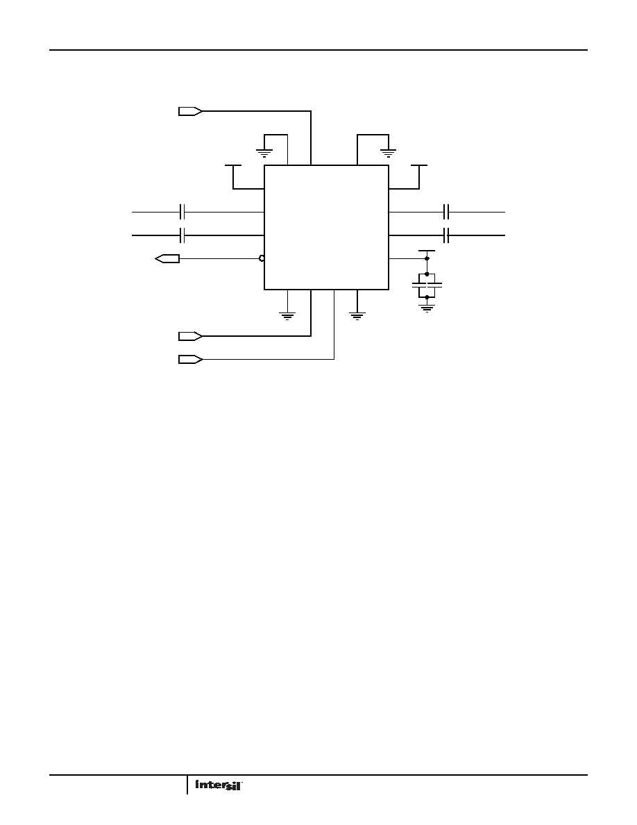
Typical application schematic for ISL36111 is shown in Figure 8.
PCB Layout Considerations
Because of the high speed of the ISL36111 signals, careful PCB
layout is critical to maximize performance. The following
guidelines should be adhered to as closely as possible:
All high speed differential pair traces should have a
characteristic impedance of 50
Ω with respect to ground plane
and 100
Ω with respect to each other.
Avoid using vias for high speed traces as this will create
discontinuity in the traces characteristic impedance.
Input and output traces need to have DC blocking capacitors
(100nF). Capacitors should be placed as close to the chip as
possible.
For each differential pair, the positive trace and the negative
trace need to be of same length in order to avoid intra-pair
skew. Serpentine technique may be used to match trace
lengths.
Maintain a constant solid ground plane underneath the high-
speed differential traces
Each VDD pin should be connected to 1.2V and also bypassed
to ground through a 47nF and a 100pF capacitor in parallel.
Minimize the trace length and avoid vias between the VDD pin
and the bypass capacitors in order to maximize the power
supply noise rejection.
About Q:ACTIVE
Intersil has long realized that to enable the complex server
clusters of next generation datacenters, it is critical to manage
the signal integrity issues of electrical interconnects. To address
this, Intersil has developed its groundbreaking Q:ACTIVE
product line. By integrating its analog ICs inside cabling
interconnects, Intersil is able to achieve unsurpassed
improvements in reach, power consumption, latency, and cable
gauge size as well as increased airflow in tomorrow’s
datacenters. This new technology transforms passive cabling into
intelligent “roadways” that yield lower operating expenses and
capital expenditures for the expanding datacenter.
Intersil Lane Extenders allow greater reach over existing cabling
while reducing the need for thicker cables. This significantly
reduces cable weight and clutter, increases airflow, and improves
power consumption.
FIGURE 8. TYPICAL APPLICATION REFERENCE SCHEMATIC FOR ISL36111
NOTES:
14. See “Control Pin Boost Setting” on page 5 for information on how to connect the CP pins
15. See “Detection Thereshold (DT) Pin Functionality” on page 6 for details on DT pin operation.
16. Although the filtering network is shown only for one VDD pin for simplicity, all the VDD pins need to be connected in this way.
DT
CPA
CPB
LOSB (output)
1.2V
47nF
ISL36111
IN_P
2
IN_N
3
DT
15
VDD
1
VDD
9
VDD
12
OUT_N
10
OUT_P
11
NC
14
LOSB
4
GND
16
GND
5
CP
A
6
CPB
7
GND
8
GND
13
100nF
100pF
100nF
INPUT SIGNAL
OUTPUT SIGNAL
相关PDF资料 |
PDF描述 |
|---|---|
| M3CKK-1620K | IDC CABLE - MKC16K/MC16F/MPK16K |
| ISL35411DRZ-EVALZ | EVAL BAORD FOR ISL35411DRZ |
| ISL35111DRZ-EVALZ | EVAL BAORD FOR ISL35111DRZ |
| EBL4270-EVALZ | EVAL BOARD FOR QLX4270 |
| ECM28DCCS-S189 | CONN EDGECARD 56POS R/A .156 SLD |
相关代理商/技术参数 |
参数描述 |
|---|---|
| ISL36111DRZ-T7 | 功能描述:IC EQUALIZER REC 11.1GBPS 16QFN RoHS:是 类别:集成电路 (IC) >> 接口 - 专用 系列:QLx™ 特色产品:NXP - I2C Interface 标准包装:1 系列:- 应用:2 通道 I²C 多路复用器 接口:I²C,SM 总线 电源电压:2.3 V ~ 5.5 V 封装/外壳:16-TSSOP(0.173",4.40mm 宽) 供应商设备封装:16-TSSOP 包装:剪切带 (CT) 安装类型:表面贴装 产品目录页面:825 (CN2011-ZH PDF) 其它名称:568-1854-1 |
| ISL36111DRZ-TS | 功能描述:IC EQUALIZER REC 11.1GBPS 16QFN RoHS:是 类别:集成电路 (IC) >> 接口 - 专用 系列:QLx™ 标准包装:3,000 系列:- 应用:PDA,便携式音频/视频,智能电话 接口:I²C,2 线串口 电源电压:1.65 V ~ 3.6 V 封装/外壳:24-WQFN 裸露焊盘 供应商设备封装:24-QFN 裸露焊盘(4x4) 包装:带卷 (TR) 安装类型:表面贴装 产品目录页面:1015 (CN2011-ZH PDF) 其它名称:296-25223-2 |
| ISL36356A-APDK | 制造商:INTERSIL 制造商全称:Intersil Corporation 功能描述:PRISM 11Mbps Wireless Local Area Network Access Point |
| ISL36356A-APDK-EVAL | 制造商:INTERSIL 制造商全称:Intersil Corporation 功能描述:PRISM 11Mbps Wireless Local Area Network Access Point |
| ISL36411 | 制造商:INTERSIL 制造商全称:Intersil Corporation 功能描述:Quad Lane Extender |
发布紧急采购,3分钟左右您将得到回复。