- 您现在的位置:买卖IC网 > PDF目录11427 > ISL43121IHZ-T (Intersil)IC SWITCH DUAL SPST SOT23-8 PDF资料下载
参数资料
| 型号: | ISL43121IHZ-T |
| 厂商: | Intersil |
| 文件页数: | 6/12页 |
| 文件大小: | 0K |
| 描述: | IC SWITCH DUAL SPST SOT23-8 |
| 标准包装: | 1 |
| 功能: | 开关 |
| 电路: | 2 x SPST - NC |
| 导通状态电阻: | 20 欧姆 |
| 电压电源: | 单电源 |
| 电压 - 电源,单路/双路(±): | 2.7 V ~ 12 V |
| 电流 - 电源: | 1µA |
| 工作温度: | -40°C ~ 85°C |
| 安装类型: | 表面贴装 |
| 封装/外壳: | SOT-23-8 |
| 供应商设备封装: | SOT-23-8 |
| 包装: | 标准包装 |
| 其它名称: | ISL43121IHZ-DKR ISL43121IHZ-DKR-ND ISL43121IHZDKR |
3
FN6033.5
October 18, 2007
Absolute Maximum Ratings
Thermal Information
V+ to GND . . . . . . . . . . . . . . . . . . . . . . . . . . . . . . . . . . -0.3V to 15V
Input Voltages
IN (Note 2). . . . . . . . . . . . . . . . . . . . . . . . . . -0.3V to ((V+) + 0.3V)
NO, NC (Note 2) . . . . . . . . . . . . . . . . . . . . . -0.3V to ((V+) + 0.3V)
Output Voltages
COM (Note 2) . . . . . . . . . . . . . . . . . . . . . . . -0.3V to ((V+) + 0.3V)
Continuous Current (Any Terminal) . . . . . . . . . . . . . . . . . . . . .
30mA
Peak Current NO, NC, or COM
(Pulsed 1ms, 10% Duty Cycle, Max) . . . . . . . . . . . . . . . . . .
40mA
ESD Rating
Human Body Model (Per MIL-STD-883 Method 3015) . . . . .>2kV
Operating Conditions
Temperature Range
ISL43XXXIH-T . . . . . . . . . . . . . . . . . . . . . . . . . . . . . -40°C to +85°C
Thermal Resistance (Typical, Note 3)
θ
JA (°C/W)
8 Ld SOT-23 Package . . . . . . . . . . . . . . . . . . . . . . .
215
Maximum Junction Temperature (Plastic Package). . . . . . . +150°C
Maximum Storage Temperature Range . . . . . . . . . . . -65°C to +150°C
Pb-free reflow profile . . . . . . . . . . . . . . . . . . . . . . . . . .see link below
CAUTION: Do not operate at or near the maximum ratings listed for extended periods of time. Exposure to such conditions may adversely impact product reliability and
result in failures not covered by warranty.
NOTES:
2. Signals on NC, NO, COM, or IN exceeding V+ or GND are clamped by internal diodes. Limit forward diode current to maximum current ratings.
3.
θ
JA is measured with the component mounted on a low effective thermal conductivity test board in free air. See Tech Brief TB379 for details.
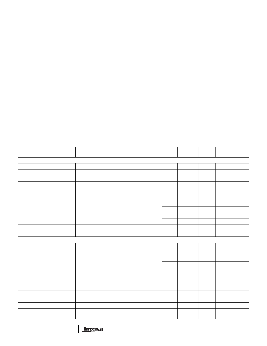
Electrical Specifications - 5V Supply
Unless Otherwise Specified.
PARAMETER
TEST CONDITIONS
TEMP
(°C)
MIN
(Notes 5, 6)
TYP
MAX
(Notes 5, 6) UNITS
ANALOG SWITCH CHARACTERISTICS
Analog Signal Range, VANALOG
Full
0
-
V+
V
ON-Resistance, rON
V+ = 4.5V, ICOM = 1.0mA, VNO or VNC = 3.5V
(See Figure 5)
25
-
19
30
Ω
Full
-
23
40
Ω
rON Matching Between Channels,
Δr
ON
V+ = 5V, ICOM = 1.0mA, VNO or VNC = 3.5V
25
-
0.8
2
Ω
Full
-
1
4
Ω
rON Flatness, rFLAT(ON)
V+ = 5V, ICOM = 1.0mA, VNO or VNC = 1V, 2V, 3V
Full
-
7
8
Ω
NO or NC OFF Leakage Current,
INO(OFF) or INC(OFF)
V+ = 5.5V, VCOM = 1V, 4.5V, VNO or VNC = 4.5V, 1V
25
-0.1
0.01
0.1
nA
Full
-5
-
5
nA
COM OFF Leakage Current,
ICOM(OFF)
V+ = 5.5V, VCOM = 4.5V, 1V, VNO or VNC = 1V, 4.5V
25
-0.1
-
0.1
nA
Full
-5
-
5
nA
COM ON Leakage Current,
ICOM(ON)
V
+ = 5.5V, VCOM = 1V, 4.5V, or VNO or VNC = 1V, 4.5V,
or Floating
25
-0.2
-
0.2
nA
Full
-10
-
10
nA
DYNAMIC CHARACTERISTICS
Turn-ON Time, tON
VNO or VNC = 3V, RL =1kΩ, CL = 35pF, VIN = 0V to 3V
25
-
28
75
ns
Full
-
40
150
ns
Turn-OFF Time, tOFF
VNO or VNC = 3V, RL =1kΩ, CL = 35pF, VIN = 0V to 3V
25
-
20
50
ns
Full
-
30
100
ns
Break-Before-Make Time Delay
(ISL43122 only), tD
RL = 300Ω, CL = 35pF, VNO = VNC = 3V, VIN = 0V to 3V
Full
3
10
-
ns
Charge Injection, Q
25
-
3
5
pC
OFF Isolation
25
-
76
-
dB
Crosstalk (Channel-to-Channel)
25
-
-105
-
dB
Power Supply Rejection Ratio
RL = 50Ω, CL = 5pF, f = 1MHz
25
-
60
-
dB
25
-
8
-
pF
COM OFF Capacitance,
CCOM(OFF)
25
-
8
-
pF
ISL43120, ISL43121, ISL43122
相关PDF资料 |
PDF描述 |
|---|---|
| NLAS7222BMUTBG | IC USB SWITCH DPDT 10UQFN |
| ISL5123IHZ-T | IC SWITCH SPDT SOT23-6 |
| VE-23L-CV-F4 | CONVERTER MOD DC/DC 28V 150W |
| VE-23L-CV-F3 | CONVERTER MOD DC/DC 28V 150W |
| VE-23L-CV-F2 | CONVERTER MOD DC/DC 28V 150W |
相关代理商/技术参数 |
参数描述 |
|---|---|
| ISL43122 | 制造商:INTERSIL 制造商全称:Intersil Corporation 功能描述:Low-Voltage, Single Supply, Dual SPST Analog Switches |
| ISL43122IH-T | 功能描述:IC SWITCH DUAL SPST SOT23-8 RoHS:否 类别:集成电路 (IC) >> 接口 - 模拟开关,多路复用器,多路分解器 系列:- 标准包装:48 系列:- 功能:开关 电路:4 x SPST - NO 导通状态电阻:100 欧姆 电压电源:单/双电源 电压 - 电源,单路/双路(±):2 V ~ 12 V,±2 V ~ 6 V 电流 - 电源:50nA 工作温度:-40°C ~ 85°C 安装类型:表面贴装 封装/外壳:16-SOIC(0.154",3.90mm 宽) 供应商设备封装:16-SOIC 包装:管件 |
| ISL43122IHZ-T | 功能描述:IC SWITCH DUAL SPST SOT23-8 RoHS:是 类别:集成电路 (IC) >> 接口 - 模拟开关,多路复用器,多路分解器 系列:- 产品培训模块:Lead (SnPb) Finish for COTS Obsolescence Mitigation Program 标准包装:36 系列:- 功能:多路复用器 电路:2 x 4:1 导通状态电阻:75 欧姆 电压电源:单/双电源 电压 - 电源,单路/双路(±):2 V ~ 12 V,±2 V ~ 6 V 电流 - 电源:- 工作温度:0°C ~ 70°C 安装类型:表面贴装 封装/外壳:20-SOIC(0.295",7.50mm 宽) 供应商设备封装:20-SOIC W 包装:管件 |
| ISL43140 | 制造商:INTERSIL 制造商全称:Intersil Corporation 功能描述:Low-Voltage, Single and Dual Supply, High Performance, Quad SPST, Analog Switches |
| ISL43140_04 | 制造商:INTERSIL 制造商全称:Intersil Corporation 功能描述:Low-Voltage, Single and Dual Supply, High Performance, Quad SPST, Analog Switches |
发布紧急采购,3分钟左右您将得到回复。