- 您现在的位置:买卖IC网 > PDF目录11077 > ISL43140IR (Intersil)IC SWITCH QUAD SPST 16QFN PDF资料下载
参数资料
| 型号: | ISL43140IR |
| 厂商: | Intersil |
| 文件页数: | 2/16页 |
| 文件大小: | 0K |
| 描述: | IC SWITCH QUAD SPST 16QFN |
| 标准包装: | 100 |
| 功能: | 开关 |
| 电路: | 4 x SPST - NC |
| 导通状态电阻: | 65 欧姆 |
| 电压电源: | 单/双电源 |
| 电压 - 电源,单路/双路(±): | 2 V ~ 12 V,±2 V ~ 6 V |
| 电流 - 电源: | 50nA |
| 工作温度: | -40°C ~ 85°C |
| 安装类型: | 表面贴装 |
| 封装/外壳: | 16-VFQFN 裸露焊盘 |
| 供应商设备封装: | 16-QFN-EP(3x3) |
10
Detailed Description
The ISL43140–ISL43142 quad analog switches offer precise
switching capability from a bipolar ±2V to ±6V or a single 2V
to 12V supply with low on-resistance (50
) and high speed
switching (tON = 40ns, tOFF = 15ns). The devices are
especially well suited to portable battery powered equipment
thanks to the low operating supply voltage (2V), low power
consumption (1
W), low leakage currents (1nA max), and the
tiny QFN packaging. High frequency applications also benefit
from the wide bandwidth, and the very high off isolation and
crosstalk rejection.
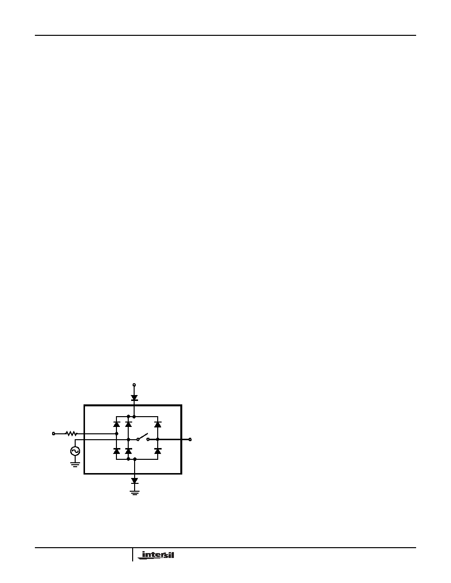
Supply Sequencing And Overvoltage Protection
With any CMOS device, proper power supply sequencing is
required to protect the device from excessive input currents
which might permanently damage the IC. All I/O pins contain
ESD protection diodes from the pin to V+ and to V- (see
Figure 8). To prevent forward biasing these diodes, V+ and
V- must be applied before any input signals, and input signal
voltages must remain between V+ and V-. If these conditions
cannot be guaranteed, then one of the following two
protection methods should be employed.
Logic inputs can easily be protected by adding a 1k
resistor in series with the input (see Figure 8). The resistor
limits the input current below the threshold that produces
permanent damage, and the sub-microamp input current
produces an insignificant voltage drop during normal
operation.
Adding a series resistor to the switch input defeats the
purpose of using a low RON switch, so two small signal
diodes can be added in series with the supply pins to provide
overvoltage protection for all pins (see Figure 8). These
additional diodes limit the analog signal from 1V below V+ to
1V above V-. The low leakage current performance is
unaffected by this approach, but the switch resistance may
increase, especially at low supply voltages.
Power-Supply Considerations
The ISL4314X construction is typical of most CMOS analog
switches, in that they have three supply pins: V+, V-, and
GND. V+ and V- drive the internal CMOS switches and set
their analog voltage limits, so there are no connections
between the analog signal path and GND. Unlike switches
with a 13V maximum supply voltage, the ISL4314X 15V
maximum supply voltage provides plenty of room for the
10% tolerance of 12V supplies (±6V or 12V single supply),
as well as room for overshoot and noise spikes.
This family of switches performs equally well when operated
with bipolar or single voltage supplies. The addition of the
GND pin allows for asymmetrical bipolar supplies (e.g. +5V
and -3V). The minimum recommended supply voltage is 2V
or ±2V. It is important to note that the input signal range,
switching times, and on-resistance degrade at lower supply
voltages. Refer to the electrical specification tables and
Typical Performance Curves for details.
V+ and GND power the internal logic (thus setting the digital
switching point) and level shifters. The level shifters convert
the logic levels to switched V+ and V- signals to drive the
analog switch gate terminals, so switch parameters -
especially RON - are strongly influenced by V-.
Logic-Level Thresholds
V+ and GND power the internal logic stages, so V- has no
affect on logic thresholds. This switch family is TTL
compatible (0.8V and 2.4V) over a V+ supply range of 2.5V
to 10V (see Figure 17). At 12V the VIH level is about 2.7V,
so for best results use a logic family the provides a VOH
greater than 3V.
The digital input stages draw supply current whenever the
digital input voltage is not at one of the supply rails. Driving
the digital input signals from GND to V+ with a fast transition
time minimizes power dissipation.
High-Frequency Performance
In 5
0 systems, signal response is reasonably flat even past
100MHz (see Figure 18). Figure 18 also illustrates that the
frequency response is very consistent over a wide V+ range,
and for varying analog signal levels.
An off switch acts like a capacitor and passes higher
frequencies with less attenuation, resulting in signal
feedthrough from a switch’s input to its output. Off Isolation
is the resistance to this feedthrough, while Crosstalk
indicates the amount of feedthrough from one switch to
another. Figure 19 details the high Off Isolation and
Crosstalk rejection provided by this family. At 10MHz, off
isolation is about 50dB in 5
0 systems, decreasing
approximately 20dB per decade as frequency increases.
Higher load impedances decrease Off Isolation and
Crosstalk rejection due to the voltage divider action of the
switch OFF impedance and the load impedance.
FIGURE 8. OVERVOLTAGE PROTECTION
V-
VCOM
VNO or NC
OPTIONAL PROTECTION
V+
INX
DIODE
OPTIONAL PROTECTION
DIODE
OPTIONAL
PROTECTION
RESISTOR
ISL43140, ISL43141, ISL43142
相关PDF资料 |
PDF描述 |
|---|---|
| ISL43121IH-T | IC SWITCH DUAL SPST SOT23-8 |
| ISL43113IB-T | IC SWITCH SPST 8SOIC |
| ISL43112IB-T | IC SWITCH SPST 8SOIC |
| ISL43110IB-T | IC SWITCH SPST 8SOIC |
| HI9P5043-5 | IC SWITCH DUAL SPDT 16SOIC |
相关代理商/技术参数 |
参数描述 |
|---|---|
| ISL43140IR-T | 功能描述:IC SWITCH QUAD SPST 16QFN RoHS:否 类别:集成电路 (IC) >> 接口 - 模拟开关,多路复用器,多路分解器 系列:- 标准包装:48 系列:- 功能:开关 电路:4 x SPST - NO 导通状态电阻:100 欧姆 电压电源:单/双电源 电压 - 电源,单路/双路(±):2 V ~ 12 V,±2 V ~ 6 V 电流 - 电源:50nA 工作温度:-40°C ~ 85°C 安装类型:表面贴装 封装/外壳:16-SOIC(0.154",3.90mm 宽) 供应商设备封装:16-SOIC 包装:管件 |
| ISL43140IRZ | 功能描述:IC SWITCH QUAD SPST 16QFN RoHS:是 类别:集成电路 (IC) >> 接口 - 模拟开关,多路复用器,多路分解器 系列:- 产品培训模块:Lead (SnPb) Finish for COTS Obsolescence Mitigation Program 标准包装:36 系列:- 功能:多路复用器 电路:2 x 4:1 导通状态电阻:75 欧姆 电压电源:单/双电源 电压 - 电源,单路/双路(±):2 V ~ 12 V,±2 V ~ 6 V 电流 - 电源:- 工作温度:0°C ~ 70°C 安装类型:表面贴装 封装/外壳:20-SOIC(0.295",7.50mm 宽) 供应商设备封装:20-SOIC W 包装:管件 |
| ISL43140IRZ-T | 功能描述:IC SWITCH QUAD SPST 16QFN RoHS:是 类别:集成电路 (IC) >> 接口 - 模拟开关,多路复用器,多路分解器 系列:- 产品培训模块:Lead (SnPb) Finish for COTS Obsolescence Mitigation Program 标准包装:36 系列:- 功能:多路复用器 电路:2 x 4:1 导通状态电阻:75 欧姆 电压电源:单/双电源 电压 - 电源,单路/双路(±):2 V ~ 12 V,±2 V ~ 6 V 电流 - 电源:- 工作温度:0°C ~ 70°C 安装类型:表面贴装 封装/外壳:20-SOIC(0.295",7.50mm 宽) 供应商设备封装:20-SOIC W 包装:管件 |
| ISL43140IV | 功能描述:IC SWITCH QUAD SPST 16TSSOP RoHS:否 类别:集成电路 (IC) >> 接口 - 模拟开关,多路复用器,多路分解器 系列:- 标准包装:48 系列:- 功能:开关 电路:4 x SPST - NO 导通状态电阻:100 欧姆 电压电源:单/双电源 电压 - 电源,单路/双路(±):2 V ~ 12 V,±2 V ~ 6 V 电流 - 电源:50nA 工作温度:-40°C ~ 85°C 安装类型:表面贴装 封装/外壳:16-SOIC(0.154",3.90mm 宽) 供应商设备封装:16-SOIC 包装:管件 |
| ISL43140IV-T | 功能描述:IC SWITCH QUAD SPST 16TSSOP RoHS:否 类别:集成电路 (IC) >> 接口 - 模拟开关,多路复用器,多路分解器 系列:- 标准包装:48 系列:- 功能:开关 电路:4 x SPST - NO 导通状态电阻:100 欧姆 电压电源:单/双电源 电压 - 电源,单路/双路(±):2 V ~ 12 V,±2 V ~ 6 V 电流 - 电源:50nA 工作温度:-40°C ~ 85°C 安装类型:表面贴装 封装/外壳:16-SOIC(0.154",3.90mm 宽) 供应商设备封装:16-SOIC 包装:管件 |
发布紧急采购,3分钟左右您将得到回复。