- 您现在的位置:买卖IC网 > PDF目录11188 > ISL43L110IHZ-T (Intersil)IC SWITCH SPST SC70-5 PDF资料下载
参数资料
| 型号: | ISL43L110IHZ-T |
| 厂商: | Intersil |
| 文件页数: | 5/11页 |
| 文件大小: | 0K |
| 描述: | IC SWITCH SPST SC70-5 |
| 标准包装: | 1 |
| 功能: | 开关 |
| 电路: | 1 x SPST- NO |
| 导通状态电阻: | 220 毫欧 |
| 电压电源: | 单电源 |
| 电压 - 电源,单路/双路(±): | 1.1 V ~ 4.5 V |
| 电流 - 电源: | 50nA |
| 工作温度: | -40°C ~ 85°C |
| 安装类型: | 表面贴装 |
| 封装/外壳: | 6-TSSOP(5 引线),SC-88A,SOT-353 |
| 供应商设备封装: | SC-70-5 |
| 包装: | 标准包装 |
| 其它名称: | ISL43L110IHZ-TDKR |
3
FN6130.0
March 15, 2005
Absolute Maximum Ratings
Thermal Information
V+ to GND . . . . . . . . . . . . . . . . . . . . . . . . . . . . . . . . . . . -0.3 to 4.7V
Input Voltages
NO, NC, IN (Note 2) . . . . . . . . . . . . . . . . . . . -0.3 to ((V+) + 0.3V)
Output Voltages
COM (Note 2) . . . . . . . . . . . . . . . . . . . . . . . . -0.3 to ((V+) + 0.3V)
Continuous Current NO, NC, or COM . . . . . . . . . . . . . . . . .
±300mA
Peak Current NO, NC, or COM
(Pulsed 1ms, 10% Duty Cycle, Max)
. . . . . . . . . . . . . . . . . ± 600mA
ESD Rating:
HBM
> . . . . . . . . . . . . . . . . . . . . . . . . . . . . . . . . . . . . . . . . . .>4kV
MM . . . . . . . . . . . . . . . . . . . . . . . . . . . . . . . . . . . . . . . . . . . .>300V
CDM . . . . . . . . . . . . . . . . . . . . . . . . . . . . . . . . . . . . . . . . . .>1000V
Operating Conditions
Temperature Range . . . . . . . . . . . . . . . . . . . . . . . . . . -40°C to 85°C
Thermal Resistance (Typical, Note 3)
θJA (°C/W)
5 Ld SC70 Package . . . . . . . . . . . . . . . . . . . . . . . . .
660
Maximum Junction Temperature (Plastic Package). . . . . . . . 150°C
Maximum Storage Temperature Range . . . . . . . . . . . . . -65°C to 150°C
Maximum Lead Temperature (Soldering 10s) . . . . . . . . . . . . 300°C
(Lead Tips Only)
CAUTION: Stresses above those listed in “Absolute Maximum Ratings” may cause permanent damage to the device. This is a stress only rating and operation of the
device at these or any other conditions above those indicated in the operational sections of this specification is not implied.
NOTES:
2. Signals on NC, NO, IN, or COM exceeding V+ or GND are clamped by internal diodes. Limit forward diode current to maximum current ratings.
3.
θJA is measured with the component mounted on a high effective thermal conductivity test board in free air. See Tech Brief TB379 for details.
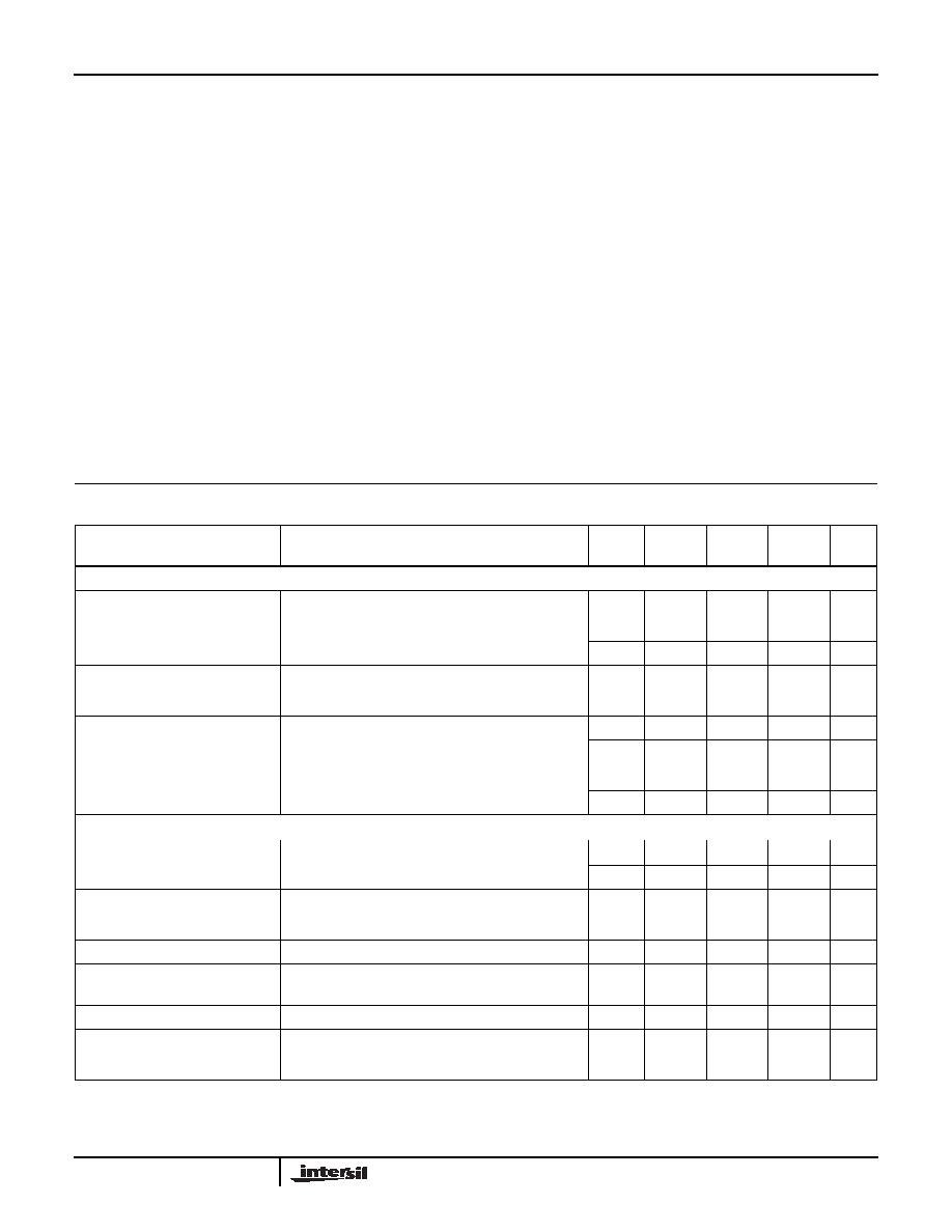
Electrical Specifications - 4.3V Supply
Test Conditions: V+ = +3.9V to +4.5V, GND = 0V, VINH = 1.6V, VINL = 0.5V (Notes 4, 6),
Unless Otherwise Specified
PARAMETER
TEST CONDITIONS
TEMP
(°C)
(NOTE 5)
MIN
TYP
(NOTE 5)
MAX
UNITS
ANALOG SWITCH CHARACTERISTICS
Analog Signal Range, VANALOG
Full
0
-
V+
V
ON Resistance, RON
V+ = 3.9V, ICOM = 100mA, VNO or VNC = 2.2V
(See Figure 4)
25
-
0.22
-
Full
-
0.25
-
RON Flatness, RFLAT(ON)
V+ = 3.9V, ICOM = 100mA, VNO or VNC = 0.8V, 2.2V,
3.5V, (Note 7)
25
-
0.03
-
Full
-
0.05
-
NO or NC OFF Leakage Current,
INO(OFF) or INC(OFF)
V+ = 4.5V, VCOM = 0.3V, 3V, VNO or VNC = 3V, 0.3V
25
-30
-
30
nA
Full
-200
-
200
nA
COM ON Leakage Current,
ICOM(ON)
V
+ = 4.5V, VCOM = 0.3V, 3V, or VNO or VNC = 0.3V, 3V,
or Floating
25
-3
-
3
nA
Full
-35
-
35
nA
DYNAMIC CHARACTERISTICS
Turn-ON Time, tON
V+ = 3.9V, VNO or VNC = 1.5V, RL = 50, CL = 35pF
(See Figure 1, Note 8)
25
-
8
15
ns
Full
-
20
ns
Turn-OFF Time, tOFF
V+ = 3.9V, VNO or VNC = 1.5V, RL = 50, CL = 35pF
(See Figure 1, Note 8)
25
-
5
10
ns
Full
-
15
ns
Charge Injection, Q
VG = V+/2, RG = 0, CL = 1.0nF (See Figure 2)
25
-
89
-
pC
OFF Isolation
RL = 50, CL = 5pF, f = 100kHz, VCOM = 1VRMS,
(See Figure 3)
25
-
-65
-
dB
Total Harmonic Distortion
f = 20Hz to 20kHz, VCOM = 2VP-P, RL = 32
25
-
0.003
-
%
25
-
68
-
pF
25
-
160
-
pF
ISL43L110, ISL43L111
相关PDF资料 |
PDF描述 |
|---|---|
| ISL43L111IHZ-T | IC SWITCH SPST SC70-5 |
| VI-J3F-IW-F3 | CONVERTER MOD DC/DC 72V 100W |
| VI-J3F-IW-F2 | CONVERTER MOD DC/DC 72V 100W |
| FSA223L10X | MUX DPDT AUDIO/USB2.0 10MPAK |
| VI-J3F-IW-F1 | CONVERTER MOD DC/DC 72V 100W |
相关代理商/技术参数 |
参数描述 |
|---|---|
| ISL43L110IHZ-TTR | 制造商:Rochester Electronics LLC 功能描述: 制造商:Intersil Corporation 功能描述: |
| ISL43L111IH-T | 功能描述:IC SWITCH SPST SC70-5 RoHS:否 类别:集成电路 (IC) >> 接口 - 模拟开关,多路复用器,多路分解器 系列:- 标准包装:48 系列:- 功能:开关 电路:4 x SPST - NO 导通状态电阻:100 欧姆 电压电源:单/双电源 电压 - 电源,单路/双路(±):2 V ~ 12 V,±2 V ~ 6 V 电流 - 电源:50nA 工作温度:-40°C ~ 85°C 安装类型:表面贴装 封装/外壳:16-SOIC(0.154",3.90mm 宽) 供应商设备封装:16-SOIC 包装:管件 |
| ISL43L111IHZ-T | 功能描述:IC SWITCH SPST SC70-5 RoHS:是 类别:集成电路 (IC) >> 接口 - 模拟开关,多路复用器,多路分解器 系列:- 产品培训模块:Lead (SnPb) Finish for COTS Obsolescence Mitigation Program 标准包装:36 系列:- 功能:多路复用器 电路:2 x 4:1 导通状态电阻:75 欧姆 电压电源:单/双电源 电压 - 电源,单路/双路(±):2 V ~ 12 V,±2 V ~ 6 V 电流 - 电源:- 工作温度:0°C ~ 70°C 安装类型:表面贴装 封装/外壳:20-SOIC(0.295",7.50mm 宽) 供应商设备封装:20-SOIC W 包装:管件 |
| ISL43L120 | 制造商:INTERSIL 制造商全称:Intersil Corporation 功能描述:Ultra Low ON-Resistance, Single Supply, Dual SPST Analog Switches |
| ISL43L120_06 | 制造商:INTERSIL 制造商全称:Intersil Corporation 功能描述:Ultra Low ON-Resistance, Single Supply, Dual SPST Analog Switches |
发布紧急采购,3分钟左右您将得到回复。