- 您现在的位置:买卖IC网 > PDF目录383132 > ISL51002EVALZ (Intersil Corporation) 10-Bit Video Analog Front End (AFE) with Measurement and Auto-Adjust Features PDF资料下载
参数资料
| 型号: | ISL51002EVALZ |
| 厂商: | Intersil Corporation |
| 英文描述: | 10-Bit Video Analog Front End (AFE) with Measurement and Auto-Adjust Features |
| 中文描述: | 10位的测量和自动视频模拟前端(AFE),调节功能 |
| 文件页数: | 8/32页 |
| 文件大小: | 360K |
| 代理商: | ISL51002EVALZ |
第1页第2页第3页第4页第5页第6页第7页当前第8页第9页第10页第11页第12页第13页第14页第15页第16页第17页第18页第19页第20页第21页第22页第23页第24页第25页第26页第27页第28页第29页第30页第31页第32页
8
December 22, 2006
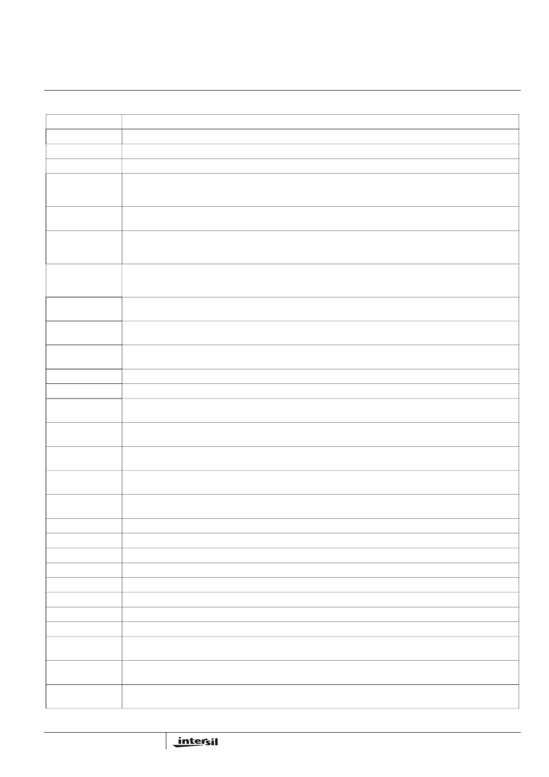
Pin Description
SYMBOL
DESCRIPTION
R
IN
0, 1, 2, 3
Analog inputs. Red channels. AC couple through 0.1μF.
G
IN
0, 1, 2, 3
Analog inputs. Green channels. AC couple through 0.1μF.
B
IN
0, 1, 2, 3
Analog inputs. Blue channels. AC couple through 0.1μF.
VREF
RED
,
VREF
GREEN
,
VREF
BLUE
Analog inputs. Reference voltage for ADCs. Tie to 1.8V reference voltage (V
A1.8
is acceptable if low noise). Decouple with
0.1μF capacitor to GND
A
.
SOG
IN
0, 1, 2, 3
Analog inputs. Sync on Green. Connect to corresponding Green channel video source through a 0.01μF capacitor in
series with a 500
Ω
resistor.
HSYNC
IN
0, 1, 2, 3
Digital
high impedance
3.3V inputs with 240mV hysteresis. Connect to corresponding channel's HSYNC source. For 5V
signals divide input with a 1k/1.9k divider. Place the divider as close as possible to the device pin. Place a 50pFcapacitor
in parallel with the 1k resistor to reduce the filtering effect of the divider.
VSYNC
IN
0, 1, 2, 3
Digital
high impedance
3.3V inputs with 240mV hysteresis. Connect to corresponding channel's VSYNC source. For 5V
signals divide input with a 1k/1.9k divider. Place the divider as close as possible to the device pin. Place a 50pF capacitor
in parallel with the 1k resistor to reduce the filtering effect of the divider.
COAST
IN
Digital 3.3V input. When this input is high and external COAST is selected, the PLL will coast, ignoring all transistions on
the active channel’s HSYNC/SOG.
CLAMP
IN
Digital 3.3V input.When this input is high and external CLAMP is selected, connects the selected channels inputs to the
clamp DAC.
CLOCKINV
IN
Digital 3.3V input. When high, changes the pixel sampling phase by +180°. Toggle at frame rate during VSYNC to allow
2x undersampling to sample odd and even pixels on sequential frames. Tie to D
GND
if unused.
FBC
IN
Digital 3.3V input.Connect to the Fast Blank signal of a SCART connector.
FBC
OUT
3.3V digital output. A delayed version of the FBC
IN
signal, aligned with the digital pixel data.
RESET
Digital 3.3V input, active low, 70k
Ω
pullup to V
D
. Take low for at least 1μs and then high again to reset the ISL51002. This
pin is not necessary for normal use and may be tied directly to the V
D
supply.
XTAL
IN
Analog input. Connect to external 12MHz to 27MHz crystal and load capacitor (see crystal spec for recommended
loading). Typical oscillation amplitude is 1.0V
P-P
centered around 0.5V.
XTAL
OUT
Analog output. Connect to external 12MHz to 27MHz crystal and load capacitor (see crystal spec for recommended
loading). Typical oscillation amplitude is 1.0V
P-P
centered around 0.5V.
XCLK
OUT
3.3V digital output. Buffered crystal clock output at f
XTAL
or f
XTAL
/2. May be used as system clock for other system
components.
SADDR
Digital 3.3V input. Address = 0x98 (1001100x) when tied low.
Address = 0 x 9A (1001101x) when tied high.
SCL
Digital input, 5V tolerant, 500mV hysteresis. Serial data clock for 2-wire interface.
SDA
Bidirectional Digital I/O, open drain, 5V tolerant. Serial data I/O for 2-wire interface.
EXTCLK
IN
Digital 3.3V input. External clock input for AFE.
R[9:0]
3.3V digital output. 10-bit Red channel pixel data.
G[9:0]
3.3V digital output. 10-bit Green channel pixel data.
B[9:0]
3.3V digital output. 10-bit Blue channel pixel data.
DATACLK
3.3V digital output. Data (pixel) clock output.
DATACLK
3.3V digital output. Inverse of DATACLK.
HS
OUT
3.3V digital output. HSYNC output aligned with pixel data. Use this output to frame the digital output data. This output is
always purely horizontal sync (without any composite sync signals)
HSYNC
OUT
3.3V digital output. Buffered HSYNC (or SOG or CSYNC) output. This is typically used for measuring HSYNC period. This
output will pass composite sync signals and Macrovision signals if present on HSYNC
IN
or SOG
IN
.
VSYNC
OUT
3.3V digital output. Buffered VSYNC output. For composite sync signals, this output will be asserted for the duration of the
disruption of the normal HSYNC pattern. This is typically used for measuring VSYNC period.
ISL51002
相关PDF资料 |
PDF描述 |
|---|---|
| ISL51002 | 10-Bit Video Analog Front End (AFE) with Measurement and Auto-Adjust Features(具有测量和音频调节功能的10-Bit视频模拟前端(AFE)) |
| ISL5120IHZ-T | Low-Voltage, Single Supply, Dual SPST, SPDT Analog Switches |
| ISL5120IH-T | Low-Voltage, Single Supply, Dual SPST, SPDT Analog Switches |
| ISL5120IB | Low-Voltage, Single Supply, Dual SPST, SPDT Analog Switches |
| ISL5120IBZ | Low-Voltage, Single Supply, Dual SPST, SPDT Analog Switches |
相关代理商/技术参数 |
参数描述 |
|---|---|
| ISL51002-EVALZ | 功能描述:EVAL BOARD FOR ISL51002 RoHS:是 类别:编程器,开发系统 >> 评估演示板和套件 系列:* 产品培训模块:Obsolescence Mitigation Program 标准包装:1 系列:- 主要目的:电源管理,电池充电器 嵌入式:否 已用 IC / 零件:MAX8903A 主要属性:1 芯锂离子电池 次要属性:状态 LED 已供物品:板 |
| ISL5100A | 制造商:INTERSIL 制造商全称:Intersil Corporation 功能描述:Quad 18V Pin Electronics Driver/Window Comparator |
| ISL5101IB | 制造商:Intersil Corporation 功能描述: |
| ISL5120 | 制造商:INTERSIL 制造商全称:Intersil Corporation 功能描述:Low-Voltage, Single Supply, Dual SPST, SPDT Analog Switches |
| ISL5120CB | 功能描述:IC SWITCH DUAL SPST 8SOIC RoHS:否 类别:集成电路 (IC) >> 接口 - 模拟开关,多路复用器,多路分解器 系列:- 标准包装:48 系列:- 功能:开关 电路:4 x SPST - NO 导通状态电阻:100 欧姆 电压电源:单/双电源 电压 - 电源,单路/双路(±):2 V ~ 12 V,±2 V ~ 6 V 电流 - 电源:50nA 工作温度:-40°C ~ 85°C 安装类型:表面贴装 封装/外壳:16-SOIC(0.154",3.90mm 宽) 供应商设备封装:16-SOIC 包装:管件 |
发布紧急采购,3分钟左右您将得到回复。