参数资料
| 型号: | ISL54053IRUZ-T |
| 厂商: | Intersil |
| 文件页数: | 6/12页 |
| 文件大小: | 0K |
| 描述: | IC SWITCH SPDT 6UTDFN |
| 标准包装: | 3,000 |
| 功能: | 开关 |
| 电路: | 1 x SPDT |
| 导通状态电阻: | 860 毫欧 |
| 电压电源: | 单电源 |
| 电压 - 电源,单路/双路(±): | 1.8 V ~ 5.5 V |
| 电流 - 电源: | 75nA |
| 工作温度: | -40°C ~ 85°C |
| 安装类型: | 表面贴装 |
| 封装/外壳: | 6-UFDFN |
| 供应商设备封装: | 6-UTDFN(1.2x1.0) |
| 包装: | 带卷 (TR) |
3
FN6460.3
October 19, 2009
Absolute Maximum Ratings
Thermal Information
V+ to GND . . . . . . . . . . . . . . . . . . . . . . . . . -0.5V to 6.5V
Input Voltages
NO, NC, IN (Note 6) . . . . . . . . . . . . -0.5 to ((V+) + 0.5V)
Output Voltages
COM (Note 6) . . . . . . . . . . . . . . . . -0.5 to ((V+) + 0.5V)
Continuous Current NO, NC, or COM. . . . . . . . . . . . ±300mA
Peak Current NO, NC, or COM
(Pulsed 1ms, 10% Duty Cycle, Max) . . . . . . . . . . ±500mA
ESD Rating
Human Body Model . . . . . . . . . . . . . . . . . . . . . . . . >6kV
Machine Model . . . . . . . . . . . . . . . . . . . . . . . . . . >200V
Charged Device Model . . . . . . . . . . . . . . . . . . . . .>2.2kV
Thermal Resistance (Typical)
θJA (°C/W) θJC (°C/W)
6 Ld TDFN (Note 7) . . . . . . . . . .
175
N/A
6 Ld SOT-23 (Notes 7, 8) . . . . . . .
260
120
Maximum Junction Temperature (Plastic Package). . +150°C
Maximum Storage Temperature Range. . . . . -65°C to +150°C
Pb-Free Reflow Profile . . . . . . . . . . . . . . . . . .see link below
http://www.intersil.com/pbfree/Pb-FreeReflow.asp
Operating Conditions
V+ (Positive DC Supply Voltage) . . . . . . . . . . . 1.8V to 5.5V
Analog Signal Range . . . . . . . . . . . . . . . . . . . . . . 0V to V+
VIN (Digital Logic Input Voltage (IN) . . . . . . . . . . . 0V to V+
Temperature Range . . . . . . . . . . . . . . . . . . -40°C to +85°C
CAUTION: Do not operate at or near the maximum ratings listed for extended periods of time. Exposure to such conditions may adversely impact
product reliability and result in failures not covered by warranty.
NOTES:
6. Signals on NC, NO, IN, or COM exceeding V+ or GND are clamped by internal diodes. Limit forward diode current to maximum
current ratings.
7. θJA is measured with the component mounted on a high effective thermal conductivity test board in free air. See Tech Brief
TB379 for details.
8. For θJC, the “case temp” location is taken at the package top center.
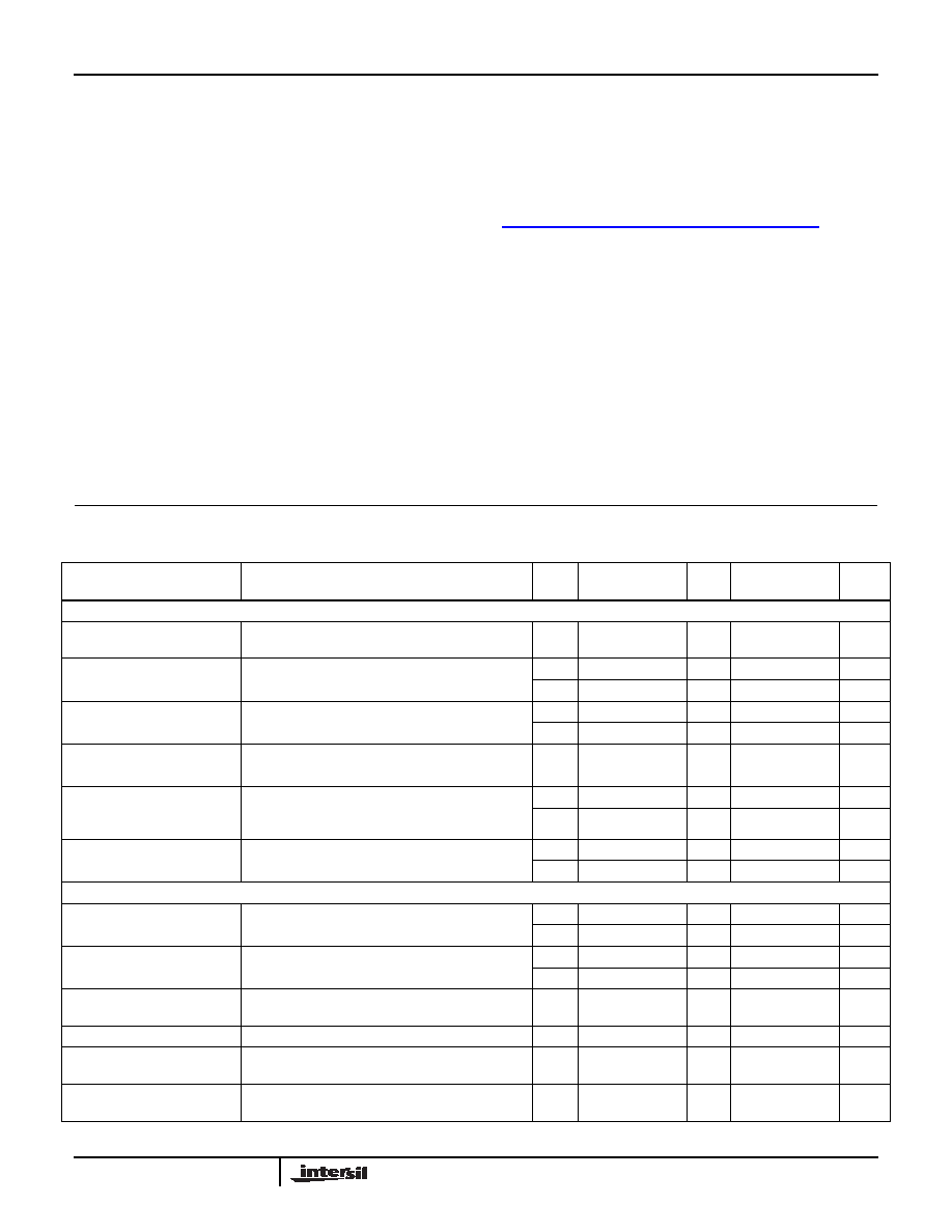
Electrical Specifications - 5V Supply Test Conditions: V+ = +4.5V to +5.5V, GND = 0V, VINH = 2.4V, VINL = 0.8V (Note 9),
Unless Otherwise Specified. Boldface limits apply over the operating temperature
range, -40°C to +85°C.
PARAMETER
TEST CONDITIONS
TEMP
(°C)
MIN
(Notes 10, 11) TYP
MAX
(Notes 10, 11) UNITS
ANALOG SWITCH CHARACTERISTICS
Analog Signal Range,
VANALOG
Full
0
-
V+
V
ON-Resistance, rON
V+ = 4.5V, ICOM = 100mA, VNO or VNC = 0V
25
-
0.86
-
Ω
Full
-
1
-
Ω
rON Matching Between
Channels, ΔrON
V+ = 4.5V, ICOM = 100mA, VNO or VNC = 2.5V,
(Note 13)
25
-
0.004
-
Ω
Full
-
0.004
-
Ω
rON Flatness, rFLAT(ON)
V+ = 4.5V, ICOM = 100mA, VNO or VNC = 0V
to V+, (Notes 12, 13)
25
-
0.25
-
Ω
Full
-
0.27
-
Ω
NO or NC OFF Leakage
Current, INO(OFF) or
INC(OFF)
V+ = 5.5V, VCOM = 0.3V, 5V, VNO or VNC = 5V,
0.3V
25
-10
5
10
nA
Full
-150
-
150
nA
COM ON Leakage Current,
ICOM(ON)
V+ = 5.5V, VCOM = 0.3V, 5V, or VNO or
VNC = 0.3V, 5V, or floating
25
-20
9
20
nA
Full
-300
-
300
nA
DYNAMIC CHARACTERISTICS
Turn-ON Time, tON
V+ = 4.5V, VNO or VNC = 3.0V, RL = 50Ω,
25
-
24
-
ns
Full
-
30
-
ns
Turn-OFF Time, tOFF
V+ = 4.5V, VNO or VNC = 3.0V, RL = 50Ω,
25
-
10
-
ns
Full
-
15
-
ns
Break-Before-Make Time
Delay, tD
V+ = 5.5V, VNO or VNC = 3.0V, RL = 50Ω,
Full
-
10
-
ns
Charge Injection, Q
25
-
26
-
pC
OFF Isolation
RL = 50Ω, CL = 5pF, f = 100kHz,
25
-
80
-
dB
Crosstalk
(Channel-to-Channel)
RL = 50Ω, CL = 5pF, f = 100kHz,
25
-
-83
-
dB
ISL54053
相关PDF资料 |
PDF描述 |
|---|---|
| ISL54055IRUZ-T | IC SWITCH SPST 6UTDFN |
| ISL54056IRUZ-T | IC SWITCH QUAD SPDT 16UTQFN |
| ISL54057IRUZ-T | IC SWITCH 4X1 16UTQFN |
| ISL54058IRUZ-T | IC SWITCH DUAL 4X1 16UTQFN |
| ISL54059IRUZ-T | IC SWITCH DUAL SPDT 10UTQFN |
相关代理商/技术参数 |
参数描述 |
|---|---|
| ISL54054 | 制造商:INTERSIL 制造商全称:Intersil Corporation 功能描述:Ultra Low ON-Resistance, Low Voltage, Single Supply, Single SPST/1:2 Distribution Analog Switch |
| ISL54054_0709 | 制造商:INTERSIL 制造商全称:Intersil Corporation 功能描述:Ultra Low ON-Resistance, Low Voltage, Single Supply, Single SPST/1:2 Distribution Analog Switch |
| ISL54054IHZ-T | 功能描述:IC SWITCH SPDT SGL SOT23-6 RoHS:是 类别:集成电路 (IC) >> 接口 - 模拟开关,多路复用器,多路分解器 系列:- 其它有关文件:STG4159 View All Specifications 标准包装:5,000 系列:- 功能:开关 电路:1 x SPDT 导通状态电阻:300 毫欧 电压电源:双电源 电压 - 电源,单路/双路(±):±1.65 V ~ 4.8 V 电流 - 电源:50nA 工作温度:-40°C ~ 85°C 安装类型:表面贴装 封装/外壳:7-WFBGA,FCBGA 供应商设备封装:7-覆晶 包装:带卷 (TR) |
| ISL54054IRUZ-T | 功能描述:IC SWITCH SPST 6UTDFN RoHS:是 类别:集成电路 (IC) >> 接口 - 模拟开关,多路复用器,多路分解器 系列:- 产品培训模块:Lead (SnPb) Finish for COTS Obsolescence Mitigation Program 标准包装:36 系列:- 功能:多路复用器 电路:2 x 4:1 导通状态电阻:75 欧姆 电压电源:单/双电源 电压 - 电源,单路/双路(±):2 V ~ 12 V,±2 V ~ 6 V 电流 - 电源:- 工作温度:0°C ~ 70°C 安装类型:表面贴装 封装/外壳:20-SOIC(0.295",7.50mm 宽) 供应商设备封装:20-SOIC W 包装:管件 |
| ISL54055 | 制造商:INTERSIL 制造商全称:Intersil Corporation 功能描述:Ultra Low ON-Resistance, Low Voltage, Single Supply, Single SPST/1:2 Distribution Analog Switch |
发布紧急采购,3分钟左右您将得到回复。