- 您现在的位置:买卖IC网 > PDF目录383134 > ISL54055IRUZ-T (INTERSIL CORP) Ultra Low ON-Resistance, Low Voltage, Single Supply, Single SPST/1:2 Distribution Analog Switch PDF资料下载
参数资料
| 型号: | ISL54055IRUZ-T |
| 厂商: | INTERSIL CORP |
| 元件分类: | 运动控制电子 |
| 英文描述: | Ultra Low ON-Resistance, Low Voltage, Single Supply, Single SPST/1:2 Distribution Analog Switch |
| 中文描述: | 1-CHANNEL, SGL POLE DOUBLE THROW SWITCH, PDSO6 |
| 封装: | 1.2 X 1.0 MM, 0.50 MM HEIGHT, ROHS COMPLIANT, PLASTIC, MO-255, UTDFN-6 |
| 文件页数: | 8/12页 |
| 文件大小: | 355K |
| 代理商: | ISL54055IRUZ-T |
8
FN6461.0
March 21, 2007
Power-Supply Considerations
The construction of the ISL54054 and the ISL54055 is
typical of most single supply CMOS analog switches in that
they have two supply pins: V+ and GND. V+ and GND drive
the internal CMOS switches and set their analog voltage
limits. Unlike switches with a 4.5V maximum supply voltage,
the ISL54054 and the ISL54055’s 5.5V maximum supply
voltage provides plenty of room for the 10% tolerance of
4.5V supplies, as well as room for overshoot and noise
spikes.
The minimum recommended supply voltage is 1.8V. It is
important to note that the input signal range, switching times,
and on-resistance degrade at lower supply voltages. Refer
to the electrical specification tables and
Typical Performance
Curves
on page for details.
V+ and GND also power the internal logic and level shiftier.
The level shiftier converts the input logic levels to switched
V+ and GND signals to drive the analog switch gate
terminals.
This family of switches cannot be operated with bipolar
supplies, because the input switching point becomes
negative in this configuration.
Logic-Level Thresholds
This switch family is 1.8V logic compatible (0.5V and 1.4V)
over a supply range of 2.5V to 5V (see Figure 19). At 5V the
V
IH
level is about 1.38V. This is still below the 1.8V CMOS
guaranteed high output minimum level of 1.4V, but noise
margin is reduced. At 1.8V operation the V
IL
level is around
0.1V and can only be used in 1.8V applications with minimal
ground bounce.
The digital input stages draw supply current whenever the
digital input voltage is not at one of the supply rails. Driving
the digital input signals from GND to V+ with a fast transition
time minimizes power dissipation.
High-Frequency Performance
In 50
Ω
s
ystems, the ISL54054 and the ISL54055 have a -
3dB bandwidth of 72MHz with Nx pins connected and
138MHz for a single Nx input (see Figure 20). The frequency
response is very consistent over a wide V+ range, and for
varying analog signal levels.
An OFF switch acts like a capacitor and passes higher
frequencies with less attenuation, resulting in signal
feedthrough from a switch’s input to its output. Off isolation is
the resistance to this feedthrough. Figure 21 details the high
off isolation rejection provided by this family. At 100kHz, off
isolation in 50
Ω
systems is about 74dB with Nx pins
connected and 83dB with a single Nx input, decreasing
approximately 20dB per decade as frequency increases.
Higher load impedances decrease off isolation rejection due
to the voltage divider action of the switch OFF impedance
and the load impedance.
Leakage Considerations
Reverse ESD protection diodes are internally connected
between each analog-signal pin and both V+ and GND. One of
these diodes conducts if any analog signal exceeds V+ or
GND.
Virtually all the analog leakage current comes from the ESD
diodes to V+ or GND. Although the ESD diodes on a given
signal pin are identical and therefore fairly well balanced,
they are reverse biased differently. Each is biased by either
V+ or GND and the analog signal. This means their leakages
will vary as the signal varies. The difference in the two diode
leakages to the V+ and GND pins constitutes the analog-
signal-path leakage current. All analog leakage current flows
between each pin and one of the supply terminals, not to the
other switch terminal. This is why both sides of a given
switch can show leakage currents of the same or opposite
polarity. There is no connection between the analog signal
paths and V+ or GND.
Typical Performance Curves
T
A
= +25
°
C, Unless Otherwise Specified
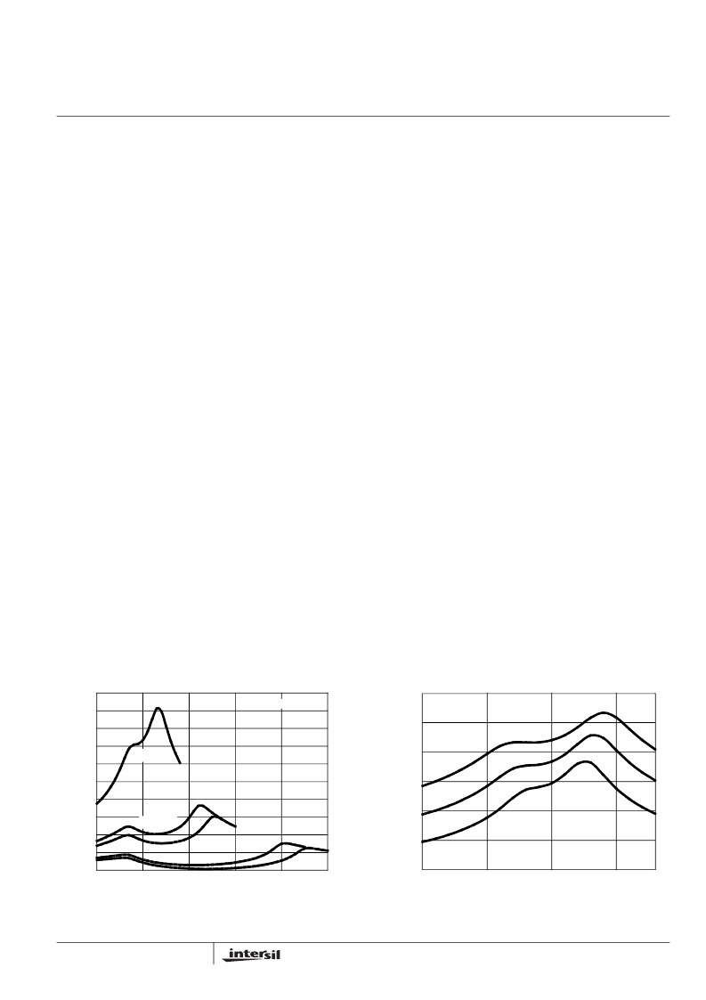
FIGURE 7. ON-RESISTANCE vs SUPPLY VOLTAGE vs
SWITCH VOLTAGE (NX PINS CONNECTED)
FIGURE 8. ON-RESISTANCE vs SWITCH VOLTAGE
(NX PINS CONNECTED)
r
O
Ω
)
V
COM
(V)
0
1
2
3
4
0.2
0.3
0.4
0.5
0.6
1.2
V+ = 2.7V
V+ = 1.8V
V+ = 4.5V
V+ = 3V
I
COM
= 100mA
V+ = 5V
5
0.7
0.8
0.9
1.0
1.1
0.2
0.4
0.6
0.8
1.0
1.2
1.4
0
0.5
1.0
1.5
1.8
r
O
Ω
)
V
COM
(V)
+25°C
+85°C
-40°C
V+ = 1.8V
I
COM
= 100mA
ISL54054, ISL54055
相关PDF资料 |
PDF描述 |
|---|---|
| ISL54056IRUZ-T | Ultra Low ON-Resistance, +1.65V to +4.5V, Single Supply, Quad SPDT (Dual DPDT) Analog Switch |
| ISL54056 | Ultra Low ON-Resistance, +1.65V to +4.5V, Single Supply, Quad SPDT (Dual DPDT) Analog Switch(超低导通电阻, +1.65V到+4.5V, 单电源, 四路单刀双掷(双路单刀双掷)模拟开关) |
| ISL54057IRUZ-T | Ultra Low ON-Resistance, Low-Voltage, Single Supply, Differential 4 to 1 Analog Multiplexer |
| ISL54057 | Ultra Low ON-Resistance, Low-Voltage, Single Supply, Differential 4 to 1 Analog Multiplexer(超低导通电阻, 低电压, 单电源, 差分4合1模拟开关) |
| ISL54058IRUZ-T | Ultra Low ON-Resistance, Low-Voltage, Single Supply, Dual 4 to 1 Analog Multiplexer |
相关代理商/技术参数 |
参数描述 |
|---|---|
| ISL54056 | 制造商:INTERSIL 制造商全称:Intersil Corporation 功能描述:Ultra Low ON-Resistance, +1.65V to +4.5V, Single Supply, Quad SPDT (Dual DPDT) Analog Switch |
| ISL54056_07 | 制造商:INTERSIL 制造商全称:Intersil Corporation 功能描述:Ultra Low ON-Resistance, +1.65V to +4.5V, Single Supply, Quad SPDT (Dual DPDT) Analog Switch |
| ISL54056IRUZ-T | 功能描述:IC SWITCH QUAD SPDT 16UTQFN RoHS:是 类别:集成电路 (IC) >> 接口 - 模拟开关,多路复用器,多路分解器 系列:- 产品培训模块:Lead (SnPb) Finish for COTS Obsolescence Mitigation Program 标准包装:36 系列:- 功能:多路复用器 电路:2 x 4:1 导通状态电阻:75 欧姆 电压电源:单/双电源 电压 - 电源,单路/双路(±):2 V ~ 12 V,±2 V ~ 6 V 电流 - 电源:- 工作温度:0°C ~ 70°C 安装类型:表面贴装 封装/外壳:20-SOIC(0.295",7.50mm 宽) 供应商设备封装:20-SOIC W 包装:管件 |
| ISL54057 | 制造商:INTERSIL 制造商全称:Intersil Corporation 功能描述:Ultra Low ON-Resistance, Low-Voltage, Single Supply, Differential 4 to 1 Analog Multiplexer |
| ISL54057IRUZ-T | 功能描述:IC SWITCH 4X1 16UTQFN RoHS:是 类别:集成电路 (IC) >> 接口 - 模拟开关,多路复用器,多路分解器 系列:- 产品培训模块:Lead (SnPb) Finish for COTS Obsolescence Mitigation Program 标准包装:36 系列:- 功能:多路复用器 电路:2 x 4:1 导通状态电阻:75 欧姆 电压电源:单/双电源 电压 - 电源,单路/双路(±):2 V ~ 12 V,±2 V ~ 6 V 电流 - 电源:- 工作温度:0°C ~ 70°C 安装类型:表面贴装 封装/外壳:20-SOIC(0.295",7.50mm 宽) 供应商设备封装:20-SOIC W 包装:管件 |
发布紧急采购,3分钟左右您将得到回复。