- 您现在的位置:买卖IC网 > PDF目录383134 > ISL54200_07 (Intersil Corporation) USB 2.0 High/Full Speed Multiplexer PDF资料下载
参数资料
| 型号: | ISL54200_07 |
| 厂商: | Intersil Corporation |
| 英文描述: | USB 2.0 High/Full Speed Multiplexer |
| 中文描述: | USB2.0高/全速多路复用器 |
| 文件页数: | 3/16页 |
| 文件大小: | 1115K |
| 代理商: | ISL54200_07 |
3
FN6408.1
July 11, 2007
Absolute Maximum Ratings
Thermal Information
VDD to GND . . . . . . . . . . . . . . . . . . . . . . . . . . . . . . . . -0.3V to 6.0V
Input Voltages
FSD2, FSD1, HSD2, HSD1 (Note 2) . . . . . - 1V to ((V
DD
) +0.3V)
IN, EN (Note 2). . . . . . . . . . . . . . . . . . . . . -0.3V to ((V
DD
) +0.3V)
Output Voltages
COMD1, COMD2 (Note 2) . . . . . . . . . . . . . . . . . . . . . . . -1V to 5V
Continuous Current (HSD2, HSD1, FSD2, FSD1). . . . . . . . . ±40mA
Peak Current (HSD2, HSD1, FSD2, FSD1)
(Pulsed 1ms, 10% Duty Cycle, Max) . . . . . . . . . . . . . . . . ±100mA
ESD Rating:
HBM . . . . . . . . . . . . . . . . . . . . . . . . . . . . . . . . . . . . . . . . . . . .>7kV
MM . . . . . . . . . . . . . . . . . . . . . . . . . . . . . . . . . . . . . . . . . . .>400V
CDM. . . . . . . . . . . . . . . . . . . . . . . . . . . . . . . . . . . . . . . . . . >1.4kV
Thermal Resistance (Typical, Note 3)
10 Ld 3x3 TDFN Package . . . . . . . . . . . . . . . . . . . .
10 Ld μTQFN Package . . . . . . . . . . . . . . . . . . . . . .
Maximum Junction Temperature (Plastic Package). . . . . . . +150°C
Maximum Storage Temperature Range . . . . . . . . . . . -65°C to +150°C
Pb-free reflow profile . . . . . . . . . . . . . . . . . . . . . . . . . .see link below
http://www.intersil.com/pbfree/Pb-FreeReflow.asp
θ
JA
(°C/W)
55
140
Operating Conditions
Temperature Range
ISL54200IRZ and ISL54200IRUZ . . . . . . . . . . . . . . -40°C to +85°C
V
DD
Supply Voltage Range. . . . . . . . . . . . . . . . . . . . . 2.7V to 5.5V
CAUTION: Do not operate at or near the maximum ratings listed for extended periods of time. Exposure to such conditions may adversely impact product reliability and
result in failures not covered by warranty.
NOTES:
2. Signals on FSD1, FSD2, HSD1, HSD2, COMD1, COMD2, EN, IN exceeding V
DD
or GND by specified amount are clamped. Limit current to
maximum current ratings.
3.
θ
JA
is measured with the component mounted on a high effective thermal conductivity test board in free air. See Tech Brief TB379 for details.
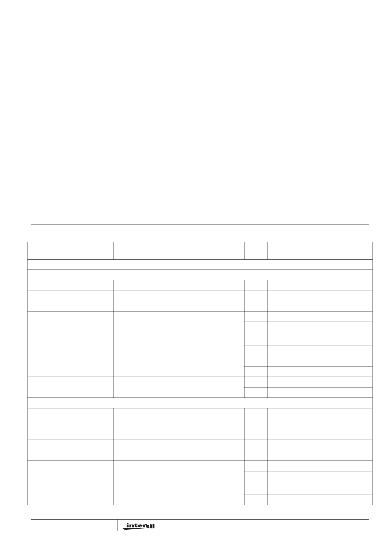
Electrical Specifications - 2.7V to 3.6V Supply
Test Conditions: V
DD
= +3.3V, GND = 0V, V
INH
= 1.4V, V
INL
= 0.5V, V
ENH
= 1.4V,
V
ENL
= 0.5V, (Note 4), Unless Otherwise Specified.
PARAMETER
TEST CONDITIONS
TEMP
(°C)
MIN
(Notes 5, 6)
TYP
MAX
(Notes 5, 6)
UNITS
ANALOG SWITCH CHARACTERISTICS
NC Switches (FSD1, FSD2)
Analog Signal Range, V
ANALOG
V
DD
= 3.3V, IN = 0V, EN = 3.3V
Full
0
-
V
DD
V
ON-Resistance, r
ON
V
DD
= 3.3V, IN = 0.5V, EN = 1.4V, I
COMx
= 40mA,
V
FSD1
or V
FSD2
= 0V to 3.3V, (See Figure 4)
+25
-
7
10
Ω
Full
-
-
15
Ω
r
ON
Matching Between Channels,
Δ
r
ON
V
DD
= 3.3V, IN = 0.5V, EN = 1.4V, I
COMx
= 40mA,
V
FSD1
or V
FSD2
= Voltage at max r
ON
over signal range
of 0V to 3.3V, (Note 8)
+25
-
0.1
0.35
Ω
Full
-
-
0.4
Ω
r
ON
Flatness, r
FLAT(ON)
V
DD
= 3.3V, IN = 0.5V, EN = 1.4V, I
COMx
= 40mA,
V
FSD1
or V
FSD2
= 0V to 3.3V, (Note 7)
+25
-
4
6
Ω
Full
-
-
8
Ω
OFF Leakage Current, I
FSX(OFF)
V+ = 3.6V, IN = 3.6V, EN = 0V and 3.6V, V
COMx
= 0.3V,
3V, V
FSX
= 3V, 0.3V
+25
-20
2
20
nA
Full
-70
-
70
nA
ON Leakage Current, I
FSX(ON)
V+ = 3.6V, IN = 0V, EN = 3.6V, V
COMx
= 0.3V, 3V,
V
FSX
= 0.3V, 3V
+25
-20
2
20
nA
Full
-70
-
70
nA
NO Switches (HSD1, HSD2)
Analog Signal Range, V
ANALOG
V
DD
= 3.3V, IN = 3.3V, EN = 3.3V
Full
0
-
V
DD
V
ON-Resistance, r
ON
V
DD
= 3.3V, IN = 1.4V, EN = 1.4V, I
COMx
= 1mA,
V
HSD2
or V
HSD1
= 3.3V (See Figure 3)
+25
-
20
30
Ω
Full
-
-
35
Ω
ON-Resistance, r
ON
V
DD
= 3.3V, IN = 1.4V, EN = 1.4V, I
COMx
= 40mA,
V
HSD2
or V
HSD1
= 0V to 400mV (See Figure 3)
+25
-
4.5
6
Ω
Full
-
-
8
Ω
r
ON
Matching Between Channels,
Δ
r
ON
V
DD
= 3.3V, IN = 1.4V, EN = 1.4V, I
COMx
= 40mA,
V
HSD2
or V
HSD1
= Voltage at max r
ON
, Voltage at max
r
ON
over signal range of 0V to 400mV (Note 8)
+25
-
0.01
0.1
Ω
Full
-
-
0.5
Ω
r
ON
Flatness, r
FLAT(ON)
V
DD
= 3.3V, IN = 1.4V, EN = 1.4V, I
COMx
= 40mA,
V
HSD2
or V
HSD1
= 0V to 400mV, (Note 7)
+25
-
0.4
1
Ω
Full
-
-
1.5
Ω
ISL54200
相关PDF资料 |
PDF描述 |
|---|---|
| ISL54200IRUZ-T | USB 2.0 High/Full Speed Multiplexer |
| ISL54200 | USB 2.0 High/Full Speed Multiplexer |
| ISL54200IRZ | USB 2.0 High/Full Speed Multiplexer |
| ISL54200IRZ-T | USB 2.0 High/Full Speed Multiplexer |
| ISL54400EVAL1Z | Low Voltage, Dual SPDT, USB/Audio Switches with Negative Signal Capability |
相关代理商/技术参数 |
参数描述 |
|---|---|
| ISL54200EVAL1Z | 功能描述:EVALUATION BOARD FOR ISL54200 RoHS:是 类别:编程器,开发系统 >> 评估演示板和套件 系列:- 标准包装:1 系列:PCI Express® (PCIe) 主要目的:接口,收发器,PCI Express 嵌入式:- 已用 IC / 零件:DS80PCI800 主要属性:- 次要属性:- 已供物品:板 |
| ISL54200IRUZ-T | 功能描述:IC USB SWITCH DUAL SPDT 10UTQFN RoHS:是 类别:集成电路 (IC) >> 接口 - 模拟开关,多路复用器,多路分解器 系列:- 标准包装:2,500 系列:- 功能:视频交叉点开关 电路:1 x 8:6 导通状态电阻:- 电压电源:单电源 电压 - 电源,单路/双路(±):3.135 V ~ 5.25 V 电流 - 电源:55mA 工作温度:-40°C ~ 85°C 安装类型:表面贴装 封装/外壳:24-TSSOP(0.173",4.40mm 宽) 供应商设备封装:24-TSSOP 包装:带卷 (TR) 产品目录页面:1214 (CN2011-ZH PDF) 其它名称:FMS6502MTC24XTR |
| ISL54200IRZ | 功能描述:IC USB SWITCH DUAL SPDT 10TDFN RoHS:是 类别:集成电路 (IC) >> 接口 - 模拟开关,多路复用器,多路分解器 系列:- 产品培训模块:Lead (SnPb) Finish for COTS Obsolescence Mitigation Program 标准包装:36 系列:- 功能:多路复用器 电路:2 x 4:1 导通状态电阻:75 欧姆 电压电源:单/双电源 电压 - 电源,单路/双路(±):2 V ~ 12 V,±2 V ~ 6 V 电流 - 电源:- 工作温度:0°C ~ 70°C 安装类型:表面贴装 封装/外壳:20-SOIC(0.295",7.50mm 宽) 供应商设备封装:20-SOIC W 包装:管件 |
| ISL54200IRZ-T | 功能描述:IC USB SWITCH DUAL SPDT 10TDFN RoHS:是 类别:集成电路 (IC) >> 接口 - 模拟开关,多路复用器,多路分解器 系列:- 产品培训模块:Lead (SnPb) Finish for COTS Obsolescence Mitigation Program 标准包装:36 系列:- 功能:多路复用器 电路:2 x 4:1 导通状态电阻:75 欧姆 电压电源:单/双电源 电压 - 电源,单路/双路(±):2 V ~ 12 V,±2 V ~ 6 V 电流 - 电源:- 工作温度:0°C ~ 70°C 安装类型:表面贴装 封装/外壳:20-SOIC(0.295",7.50mm 宽) 供应商设备封装:20-SOIC W 包装:管件 |
| ISL54205A | 制造商:INTERSIL 制造商全称:Intersil Corporation 功能描述:MP3/USB 2.0 High Speed Switch with Negative Signal Handling |
发布紧急采购,3分钟左右您将得到回复。