- 您现在的位置:买卖IC网 > PDF目录16358 > ISL54217EVAL1Z (Intersil)EVALUATION BOARD FOR ISL54217 PDF资料下载
参数资料
| 型号: | ISL54217EVAL1Z |
| 厂商: | Intersil |
| 文件页数: | 19/24页 |
| 文件大小: | 0K |
| 描述: | EVALUATION BOARD FOR ISL54217 |
| 标准包装: | 1 |
| 主要目的: | 接口,3:1 多路复用器 |
| 嵌入式: | 否 |
| 已用 IC / 零件: | ISL54217 |
| 主要属性: | 2 x SP3T 模拟开关 |
| 次要属性: | 2.7 V ~ 4.6 V 电源 |
| 已供物品: | 板 |
4
FN6817.4
June 17, 2010
Absolute Maximum Ratings
Thermal Information
VDD to GND. . . . . . . . . . . . . . . . . . . . . . . . . -0.3V to 5.5V
Input Voltages
1D+, 1D-, L, R, 2D+, 2D-. . . . . . . . . . . . . . . -2V to 5.5V
C0, C1 (Note 6). . . . . . . . . . . . . . . . . . . . . -0.3V to 5.5V
Output Voltages
COM-, COM+ . . . . . . . . . . . . . . . . . . . . . . . -2V to 5.5V
Continuous Current (L, R) . . . . . . . . . . . . . . . . . . . ±60mA
Peak Current (L, R)
(Pulsed 1ms, 10% Duty Cycle, Max) . . . . . . . . . ±120mA
Continuous Current (1D-, 1D+, 2D-, 2D+) . . . . . . . ±40mA
Peak Current (1D-, 1D+, 2D-, 2D+)
(Pulsed 1ms, 10% Duty Cycle, Max) . . . . . . . . . ±100mA
ESD Rating:
Human Body Model . . . . . . . . . . . . . . . . . . . . . . . . >5kV
Machine Model . . . . . . . . . . . . . . . . . . . . . . . . . . >500V
Charged Device Model . . . . . . . . . . . . . . . . . . . . . . >2kV
Latch-up Tested per JEDEC; Class II Level A . . . . . . at 85°C
Thermal Resistance (Typical)
θJA (°C/W) θJC (°C/W)
155
90
12 Ld TQFN Package (Notes 8, 9). .
58
1.0
Maximum Junction Temperature (Plastic Package). . +150°C
Maximum Storage Temperature Range. . . . . -65°C to +150°C
Pb-Free Reflow Profile . . . . . . . . . . . . . . . . . .see link below
Operating Conditions
Temperature Range . . . . . . . . . . . . . . . . . . -40°C to +85°C
Supply Voltage Range . . . . . . . . . . . . . . . . . . 2.7V to 4.6V
CAUTION: Do not operate at or near the maximum ratings listed for extended periods of time. Exposure to such conditions may adversely impact
product reliability and result in failures not covered by warranty.
NOTES:
6. Signals on C1 and C0 exceeding GND by specified amount are clamped. Limit current to maximum current ratings.
7. θJA is measured with the component mounted on a high effective thermal conductivity test board in free air. See Tech Brief
TB379 for details.
8. θJA is measured in free air with the component mounted on a high effective thermal conductivity test board with “direct attach”
features. See Tech Brief TB379.
9. For θJC, the “case temp” location is the center of the exposed metal pad on the package underside.
10. For θJC, the “case temp” location is taken at the package top center.
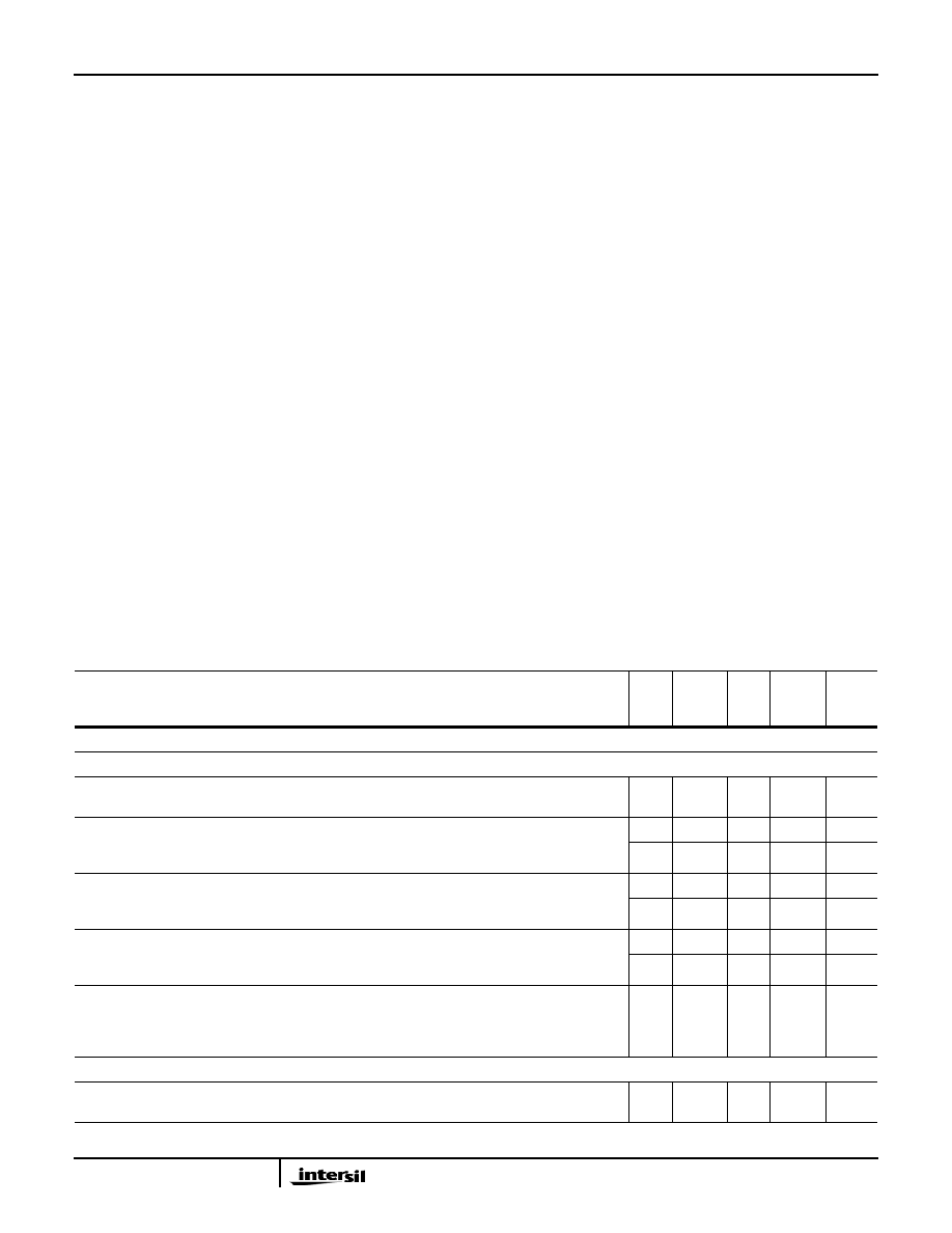
Electrical Specifications - 2.7V to 3.6V Supply Test Conditions: VDD = +3.0V, GND = 0V, VC0H, VC1H = 1.4V, VC0L,
Boldface limits apply over the operating temperature range,
-40°C to +85°C.
PARAMETER
TEST CONDITIONS
TEMP
(°C)
MIN
(Notes
12, 13) TYP
MAX
(Notes
12, 13) UNITS
ANALOG SWITCH CHARACTERISTICS
Audio Switches (L, R)
Analog Signal Range, VANALOG
VDD = 3.0V to 3.6V, Audio Mode (C0 = VDD,
C1 = VDD)
Full
-1.5
-
1.5
V
ON-Resistance, rON
VDD = 3.0V, Audio Mode (C0 = 1.4V, C1 = 1.4V),
ICOMx =60mA, VL or VR = -0.85V to 0.85V, (see
+25
-
2.3
2.8
Ω
Full
-
3.4
Ω
rON Matching Between Channels,
ΔrON
VDD = 3.0V, Audio Mode (C0 = 1.4V, C1 = 1.4V),
ICOMx =60mA, VL or VR = Voltage at max rON over
+25
-
0.04
0.25
Ω
Full
-
0.26
Ω
rON Flatness, rFLAT(ON)
VDD = 3.0V, Audio Mode (C0 = 1.4V, C1 = 1.4V),
ICOMx =60mA, VL or VR = -0.85V to 0.85V,
(Notes 14, 15)
+25
-
0.03
0.05
Ω
Full
-
0.07
Ω
Click/Pop Shunt Resistance, RL, RR VDD = 3.6V, ALL OFF Mode (C0 = 0.5V, C1 = 0.5V),
VCOM- or VCOM+ = -0.85V, 0.85V, VL or VR = -0.85V,
0.85V, Measure current into L or R pin and calculate
resistance value.
+25
-
28
-
Ω
USB/DATA Switches (1D+, 1D-, 2D+, 2D-)
Analog Signal Range, VANALOG
VDD = 2.7V to 4.6V, USB1 mode (C0 = 0V, C1 = VDD)
or USB2 Mode (C0 = VDD, C1 = 0V)
Full
-1
-
VDD
V
ISL54217
相关PDF资料 |
PDF描述 |
|---|---|
| ISL54214EVAL1Z | EVALUATION BOARD FOR ISL54214 |
| 2-1906051-3 | CA 2MM OFNR 62.5/125,LC SEC RED |
| VI-B4K-EY-S | CONVERTER MOD DC/DC 40V 50W |
| VI-B4J-EY-S | CONVERTER MOD DC/DC 36V 50W |
| VI-B43-EY-S | CONVERTER MOD DC/DC 24V 50W |
相关代理商/技术参数 |
参数描述 |
|---|---|
| ISL54217IRTZ | 功能描述:IC USB SWITCH DUAL SP3T 12TQFN RoHS:是 类别:集成电路 (IC) >> 接口 - 模拟开关,多路复用器,多路分解器 系列:- 其它有关文件:STG4159 View All Specifications 标准包装:5,000 系列:- 功能:开关 电路:1 x SPDT 导通状态电阻:300 毫欧 电压电源:双电源 电压 - 电源,单路/双路(±):±1.65 V ~ 4.8 V 电流 - 电源:50nA 工作温度:-40°C ~ 85°C 安装类型:表面贴装 封装/外壳:7-WFBGA,FCBGA 供应商设备封装:7-覆晶 包装:带卷 (TR) |
| ISL54217IRTZ-T | 功能描述:IC USB SWITCH DUAL SP3T 12TQFN RoHS:是 类别:集成电路 (IC) >> 接口 - 模拟开关,多路复用器,多路分解器 系列:- 其它有关文件:STG4159 View All Specifications 标准包装:5,000 系列:- 功能:开关 电路:1 x SPDT 导通状态电阻:300 毫欧 电压电源:双电源 电压 - 电源,单路/双路(±):±1.65 V ~ 4.8 V 电流 - 电源:50nA 工作温度:-40°C ~ 85°C 安装类型:表面贴装 封装/外壳:7-WFBGA,FCBGA 供应商设备封装:7-覆晶 包装:带卷 (TR) |
| ISL54217IRUZ-T | 功能描述:IC USB SWITCH DUAL SP3T 12UTQFN RoHS:是 类别:集成电路 (IC) >> 接口 - 模拟开关,多路复用器,多路分解器 系列:- 其它有关文件:STG4159 View All Specifications 标准包装:5,000 系列:- 功能:开关 电路:1 x SPDT 导通状态电阻:300 毫欧 电压电源:双电源 电压 - 电源,单路/双路(±):±1.65 V ~ 4.8 V 电流 - 电源:50nA 工作温度:-40°C ~ 85°C 安装类型:表面贴装 封装/外壳:7-WFBGA,FCBGA 供应商设备封装:7-覆晶 包装:带卷 (TR) |
| ISL54220 | 制造商:INTERSIL 制造商全称:Intersil Corporation 功能描述:High-Speed USB 2.0 (480Mbps) Multiplexer |
| ISL54220IRTZ | 功能描述:IC USB SWITCH DUAL SPDT 10TDFN RoHS:是 类别:集成电路 (IC) >> 接口 - 模拟开关,多路复用器,多路分解器 系列:- 应用说明:Ultrasound Imaging Systems Application Note 产品培训模块:Lead (SnPb) Finish for COTS Obsolescence Mitigation Program 标准包装:250 系列:- 功能:开关 电路:单刀单掷 导通状态电阻:48 欧姆 电压电源:单电源 电压 - 电源,单路/双路(±):2.7 V ~ 5.5 V 电流 - 电源:5µA 工作温度:0°C ~ 70°C 安装类型:表面贴装 封装/外壳:48-LQFP 供应商设备封装:48-LQFP(7x7) 包装:托盘 |
发布紧急采购,3分钟左右您将得到回复。