- 您现在的位置:买卖IC网 > PDF目录11344 > ISL54226IRUZ-T7A (Intersil)IC USB SWITCH DPST OVP 8TQFN PDF资料下载
参数资料
| 型号: | ISL54226IRUZ-T7A |
| 厂商: | Intersil |
| 文件页数: | 2/17页 |
| 文件大小: | 0K |
| 描述: | IC USB SWITCH DPST OVP 8TQFN |
| 标准包装: | 1 |
| 功能: | 开关 |
| 电路: | 2 x SPST |
| 导通状态电阻: | 17 欧姆 |
| 电压电源: | 单电源 |
| 电压 - 电源,单路/双路(±): | 2.7 V ~ 5.25 V |
| 电流 - 电源: | 45µA |
| 工作温度: | -40°C ~ 85°C |
| 安装类型: | 表面贴装 |
| 封装/外壳: | 8-XFQFN |
| 供应商设备封装: | 8-UTQFN(1.2x1.4) |
| 包装: | 标准包装 |
| 其它名称: | ISL54226IRUZ-T7ADKR |
ISL54226
10
FN7614.1
September 12, 2013
ISL54226 Operation
The following will discuss using the ISL54226 shown in the
Power
The power supply connected at the VDD pin provides the DC bias
voltage required by the ISL54226 part for proper operation. The
ISL54226 can be operated with a VDD voltage in the range of
2.7V to 5.25V.
For lowest power consumption you should use the lowest VDD
supply.
A 0.01F or 0.1F decoupling capacitor should be connected
from the VDD pin to ground to filter out any power supply noise
from entering the part. The capacitor should be located as close
to the VDD pin as possible.
In a typical application, VDD will be in the range of 2.8V to 4.3V
and will be connected to the battery or LDO of the portable
media device.
Logic Control
The state of the ISL54226 device is determined by the voltage at
the OE/ALM pin and the signal voltage at the COM pins. Refer to
The OE/ALM pin is internally pulled low through 4M resistors to
ground and can be tri-stated by a Processor.
The OE/ALM pin is an open drain connection. It should be pulled
high through an external 100k pull-up resistor. The OE/ALM pin
can then be driven “Low” by a Processor to open all switches or
it can be monitored by the Processor for a “Low” when the part
goes into an overvoltage condition.
The ISL54226 is designed to minimize IDD current consumption
when the logic control voltage is lower than the VDD supply
voltage. With VDD = 3.6V and the OE/ALM logic pin is at 1.4V the
part typically draws only 25A. With VDD = 4.3V and the OE/ALM
logic pin is at 2.6V the part typically draws only 35A. Driving the
logic pin to the VDD supply rail minimizes power consumption.
The OE/ALM pin can be driven with a voltage higher than the VDD
supply voltage. It can be driven up to 5.25V with a VDD supply in
the range of 2.7V to 5.25V.
Normal Operation Mode
With a signal level in the range of 0V to 3.6V the switches will be
ON when the OE/ALM pin = Logic “1” and will be OFF (high
impedance) when the OE/ALM pin = Logic “0”.
USB 2.0 VBUS Short Requirements
The USB specification in section 7.1.1 states a USB device must
be able to withstand a VBUS short (4.4V to 5.25V) or a -1V short to
the D+ or D- signal lines when the device is either powered off or
powered on for at least 24 hours.
The ISL54226 part has special power-off protection and OVP
detection circuitry to meet these short circuit requirements. This
circuitry allows the ISL54226 to provide protection to the USB
down-stream transceiver connected at its signal pins (D-, D+) to
meet the USB specification short circuit requirements.
The power-off protection and OVP circuitry allows the COM pins
(COM-, COM+) to be driven up to 5.25V or down to -5V while the
VDD supply voltage is in the range of 0V to 5.25V. In these
overvoltage conditions with a 500 external VDD resistor the
part draws <55A of current into the COM pins and causes no
stress/damage to the IC. In addition all switches are OFF and the
shorted VBUS voltage will be isolated from getting through to the
other side of the switch channels, thereby protecting the USB
transceiver.
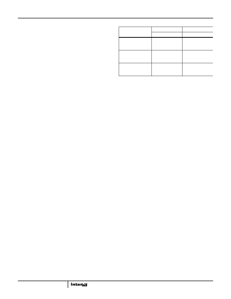
TABLE 2. LOGIC CONTROL VOLTAGE LEVELS
VDD SUPPLY RANGE
LOGIC = “0” (LOW)
LOGIC = “1” (HIGH)
OE/ALM
2.7V to 3.6V
≤0.5V
or
floating
≥1.4V
3.7V to 4.2V
≤0.7V
or
floating
≥1.7V
4.3V to 5.25V
≤0.8V
or
floating
≥2.0V
相关PDF资料 |
PDF描述 |
|---|---|
| PIC18F4610-E/P | IC MCU FLASH 32KX16 40DIP |
| DSPIC33FJ32GP202-E/SP | IC DSPIC MCU/DSP 32K 28DIP |
| VE-21J-IX-F1 | CONVERTER MOD DC/DC 36V 75W |
| VI-21J-IX-F4 | CONVERTER MOD DC/DC 36V 75W |
| PIC16C64A-10/P | IC MCU OTP 2KX14 PWM 40DIP |
相关代理商/技术参数 |
参数描述 |
|---|---|
| ISL54226IRZEVAL1Z | 制造商:INTERSIL 制造商全称:Intersil Corporation 功能描述:High-Speed USB 2.0 (480Mbps) DPST Switch with Overvoltage Protection (OVP) and Dedicated Charger Port Detection |
| ISL54227 | 制造商:INTERSIL 制造商全称:Intersil Corporation 功能描述:High-Speed USB 2.0 (480Mbps) DPST Switch with Overvoltage Protection (OVP) and Dedicated Charger Port Detection |
| ISL54227_10 | 制造商:INTERSIL 制造商全称:Intersil Corporation 功能描述:High-Speed USB 2.0 (480Mbps) DPST Switch with Overvoltage Protection (OVP) and Dedicated Charger Port Detection |
| ISL54227IRTZ | 功能描述:IC USB SWITCH DUAL DPST 10TDFN RoHS:是 类别:集成电路 (IC) >> 接口 - 模拟开关,多路复用器,多路分解器 系列:- 其它有关文件:STG4159 View All Specifications 标准包装:5,000 系列:- 功能:开关 电路:1 x SPDT 导通状态电阻:300 毫欧 电压电源:双电源 电压 - 电源,单路/双路(±):±1.65 V ~ 4.8 V 电流 - 电源:50nA 工作温度:-40°C ~ 85°C 安装类型:表面贴装 封装/外壳:7-WFBGA,FCBGA 供应商设备封装:7-覆晶 包装:带卷 (TR) |
| ISL54227IRTZEVAL1Z | 制造商:INTERSIL 制造商全称:Intersil Corporation 功能描述:High-Speed USB 2.0 (480Mbps) DPST Switch with Overvoltage Protection (OVP) and Dedicated Charger Port Detection |
发布紧急采购,3分钟左右您将得到回复。