参数资料
| 型号: | ISL54406IRTZ |
| 厂商: | Intersil |
| 文件页数: | 11/16页 |
| 文件大小: | 0K |
| 描述: | IC SWITCH DUAL SPST 10-TDFN |
| 标准包装: | 100 |
| 功能: | 开关 |
| 电路: | 2 x SPST - NO |
| 导通状态电阻: | 2.8 欧姆 |
| 电压电源: | 单电源 |
| 电压 - 电源,单路/双路(±): | 2.7 V ~ 5 V |
| 电流 - 电源: | 7µA |
| 工作温度: | -40°C ~ 85°C |
| 安装类型: | 表面贴装 |
| 封装/外壳: | 10-VFDFN 裸露焊盘 |
| 供应商设备封装: | 10-TDFN/MLP(3x3) |
| 包装: | 管件 |
| 产品目录页面: | 1247 (CN2011-ZH PDF) |
ISL54406
4
FN6578.1
July 14, 2010
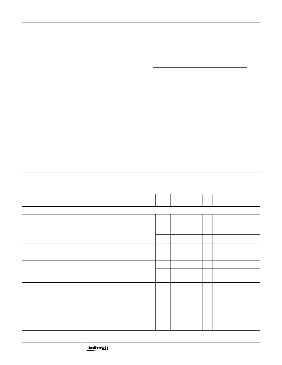
Absolute Maximum Ratings
Thermal Information
VDD to GND. . . . . . . . . . . . . . . . . . . . . . . . . . -0.3 to 5.5V
Input Voltages
Output Voltages
Continuous Current . . . . . . . . . . . . . . . . . . . . . . ±150mA
Peak Current
(Pulsed 1ms, 10% Duty Cycle, Max) . . . . . . . . . ±300mA
ESD Rating:
Human Body Model . . . . . . . . . . . . . . . . . . . . . . . . >5kV
Machine Model . . . . . . . . . . . . . . . . . . . . . . . . . . >300V
Charged Device Model . . . . . . . . . . . . . . . . . . . . .>1.5kV
Latch-up Tested per JEDEC; Class II Level A . . . . . at +85°C
Thermal Resistance (Typical)
θJA (°C/W) θJC (°C/W)
160
105
10 Ld TDFN (Notes 9, 10) . . . . . . .
55
18
Maximum Junction Temperature (Plastic Package). . +150°C
Maximum Storage Temperature Range. . . . . -65°C to +150°C
Pb-free reflow profile . . . . . . . . . . . . . . . . . . .see link below
http://www.intersil.com/pbfree/Pb-FreeReflow.asp
Operating Conditions
Temperature Range . . . . . . . . . . . . . . . . . . -40°C to +85°C
CAUTION: Do not operate at or near the maximum ratings listed for extended periods of time. Exposure to such conditions may adversely impact
product reliability and result in failures not covered by warranty.
NOTES:
6. Signals on LIN, RIN, LOUT, ROUT, SEL1, and SEL2 exceeding VDD or GND by specified amount are clamped. Limit current to
maximum current ratings.
7. θJA is measured with the component mounted on a high effective thermal conductivity test board in free air. See Tech Brief
TB379 for details.
8. For θJC, the “case temp” location is taken at the package top center.
9. θJA is measured in free air with the component mounted on a high effective thermal conductivity test board with “direct attach”
features. See Tech Brief TB379.
10. For θJC, the “case temp” location is the center of the exposed metal pad on the package underside.
Electrical Specifications - 2.7V to 3.6V Supply Test Conditions: VDD = +3.0V, GND = 0V, VSELx_H = 1.4V,
Boldface limits apply over the operating temperature range,
-40°C to +85°C.
PARAMETER
TEST CONDITIONS
TEMP
(°C)
MIN
(Notes 12, 13) TYP
MAX
ANALOG SWITCH CHARACTERISTICS
Analog Input Signal Range,
VANALOG
VDD = 3.3V, VSEL2 = 1.4V, VSEL1 = 1.4V
Full
-1.5
-
1.5
V
ON-Resistance, rON
VDD = 3.0V, VSEL2 = 1.4V, VSEL1 = 1.4V
IXOUT = 40mA, VLIN or VRIN = -0.85V to
+25
-
2.5
2.8
Ω
Full
-
4.0
Ω
rON Flatness, rFLAT(ON)
VDD = 3.0V, VSEL2 = 1.4V, VSEL1 = 1.4V
IXOUT = 40mA, VLIN or VRIN = -0.85V to
+25
-
2
-
m
Ω
Full
-
m
Ω
rON Matching Between
Channels, ΔrON
VDD = 3.0V, VSEL2 = 1.4V, VSEL1 = 1.4V
IXOUT = 40mA, VLIN or VRIN = Voltage at
max rON over signal range of -0.85V to
+25
-
0.09
0.25
Ω
Full
-
0.35
Ω
Discharge Pull-Down
Resistance, RL, RR
VDD = 3.6V, VSEL2 = 1.4V, VSEL1= 1.4V ,
VROUT or VLOUT = -0.85V, 0.85V. Measure
current through the discharge pull down
resistor and calculate resistance value.
+25
-
240
-
kΩ
Click and Pop Discharge
Resistance
VDD = 3.0V, VSEL2 = 0V, VSEL1= 1.4V,
VINL or V INR = -0.85V, 0.85V. Measure
current through the Click and Pop
discharge resistance and calculate
resistance value.
+25
-
35
-
Ω
相关PDF资料 |
PDF描述 |
|---|---|
| ISL54410IRUZ-T | IC SW USB/AUDIO DUAL SPT 10UTQFN |
| ISL54415IRUZ-T | IC USB SWITCH DUAL SPDT 10UTQFN |
| ISL54500IRUZ-T | IC SWITCH SPDT SGL 6UTDFN |
| ISL54502IHZ-T | IC SWITCH SPDT SOT23-6 |
| ISL54503IRUZ-T | IC SWITCH SPDT SGL 6UTDFN |
相关代理商/技术参数 |
参数描述 |
|---|---|
| ISL54406IRTZ-T | 功能描述:IC SWITCH DUAL SPST 10-TDFN RoHS:是 类别:集成电路 (IC) >> 接口 - 模拟开关,多路复用器,多路分解器 系列:- 标准包装:2,500 系列:- 功能:视频交叉点开关 电路:1 x 8:6 导通状态电阻:- 电压电源:单电源 电压 - 电源,单路/双路(±):3.135 V ~ 5.25 V 电流 - 电源:55mA 工作温度:-40°C ~ 85°C 安装类型:表面贴装 封装/外壳:24-TSSOP(0.173",4.40mm 宽) 供应商设备封装:24-TSSOP 包装:带卷 (TR) 产品目录页面:1214 (CN2011-ZH PDF) 其它名称:FMS6502MTC24XTR |
| ISL54406IRUZ-T | 功能描述:IC SWITCH DUAL SPST 10-TQFN RoHS:是 类别:集成电路 (IC) >> 接口 - 模拟开关,多路复用器,多路分解器 系列:- 标准包装:2,500 系列:- 功能:视频交叉点开关 电路:1 x 8:6 导通状态电阻:- 电压电源:单电源 电压 - 电源,单路/双路(±):3.135 V ~ 5.25 V 电流 - 电源:55mA 工作温度:-40°C ~ 85°C 安装类型:表面贴装 封装/外壳:24-TSSOP(0.173",4.40mm 宽) 供应商设备封装:24-TSSOP 包装:带卷 (TR) 产品目录页面:1214 (CN2011-ZH PDF) 其它名称:FMS6502MTC24XTR |
| ISL54409 | 制造商:INTERSIL 制造商全称:Intersil Corporation 功能描述:Audio/USB 2.0 Wired-OR Switch with Click and Pop Reduction |
| ISL54409_10 | 制造商:INTERSIL 制造商全称:Intersil Corporation 功能描述:Audio/USB 2.0 Wired-OR Switch with Click and Pop Reduction |
| ISL54409EVAL1Z | 功能描述:EVAL BOARD 1 FOR ISL54409 RoHS:是 类别:编程器,开发系统 >> 评估演示板和套件 系列:* 标准包装:1 系列:PCI Express® (PCIe) 主要目的:接口,收发器,PCI Express 嵌入式:- 已用 IC / 零件:DS80PCI800 主要属性:- 次要属性:- 已供物品:板 |
发布紧急采购,3分钟左右您将得到回复。