参数资料
| 型号: | ISL54505IHZ-T |
| 厂商: | Intersil |
| 文件页数: | 11/12页 |
| 文件大小: | 0K |
| 描述: | IC SWITCH SPDT SOT23-6 |
| 标准包装: | 3,000 |
| 功能: | 开关 |
| 电路: | 1 x SPST- NC |
| 导通状态电阻: | 2.5 欧姆 |
| 电压电源: | 单电源 |
| 电压 - 电源,单路/双路(±): | 1.8 V ~ 5.5 V |
| 电流 - 电源: | 28nA |
| 工作温度: | -40°C ~ 85°C |
| 安装类型: | 表面贴装 |
| 封装/外壳: | SOT-23-6 |
| 供应商设备封装: | SOT-23-6 |
| 包装: | 带卷 (TR) |
8
FN6552.2
October 23, 2009
microamp input current produces an insignificant
voltage drop during normal operation.
This method is not acceptable for the signal path
inputs. Adding a series resistor to the switch input
defeats the purpose of using a low rON switch.
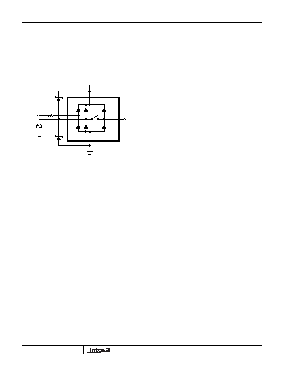
Connecting Schottky diodes to the signal pins (as
shown in Figure 7) will shunt the fault current to the
supply or to ground, thereby protecting the switch.
These Schottky diodes must be sized to handle the
expected fault current.
Power-Supply Considerations
The ISL54504, ISL54505 construction is typical of
most single supply CMOS analog switches in that they
have two supply pins: V+ and GND. V+ and GND drive
the internal CMOS switches and set their analog
voltage limits. Unlike switches with a 4V maximum
supply voltage, the ISL54504, ISL54505 5.5V
maximum supply voltage provides plenty of room for
the 10% tolerance of 3.6V supplies, as well as room for
overshoot and noise spikes.
The minimum recommended supply voltage is 1.8V but
the part will operate with a supply below 1.8V. It is
important to note that the input signal range, switching
times, and ON-resistance degrade at lower supply
voltages. Refer to the “Electrical Specifications” tables
starting on page 3 and the “Typical Performance
Curves” starting on page 9 for details.
V+ and GND also power the internal logic and level
shiftier. The level shiftier converts the input logic levels
to switched V+ and GND signals to drive the analog
switch gate terminals.
This family of switches cannot be operated with bipolar
supplies because the input switching point becomes
negative in this configuration.
Logic-Level Thresholds
This switch family is 1.8V CMOS compatible (0.5V and
1.4V) over a supply range of 2V to 3.6V (see
still below the 1.8V CMOS guaranteed high output
minimum level of 1.4V, but noise margin is reduced.
The digital input stages draw supply current whenever
the digital input voltage is not at one of the supply
rails. Driving the digital input signals from GND to V+
with a fast transition time minimizes power dissipation.
High-Frequency Performance
In 50Ω systems, the ISL54504/ISL54505 has a -3dB
bandwidth of 250MHz (see Figure 15). The frequency
response is very consistent over a wide V+ range and
for varying analog signal levels.
An OFF switch behaves like a capacitor and passes
higher frequencies with less attenuation, resulting in
signal feedthrough from a switch’s input to output. Off
isolation is the resistance of this signal feedthrough.
Figure 16 details the high off isolation provided by the
ISL54504, ISL54505. At 1MHz, off isolation is about
70dB in 50Ω systems, decreasing approximately 20dB
per decade as frequency increases. Higher load
impedances decrease off isolation due to the voltage
divider action of the switch OFF impedance and the
load impedance.
Leakage Considerations
Reverse ESD protection diodes are internally connected
between each analog-signal pin and both V+ and GND.
One of these diodes conducts if any analog signal
exceeds V+ or GND.
Virtually all the analog leakage current comes from the
ESD diodes to V+ or GND. Although the ESD diodes on
a given signal pin are identical and therefore fairly well
balanced, they are reverse biased differently. Each is
biased by either V+ or GND and the analog signal. This
means their leakages will vary as the signal varies. The
difference in the two diode leakages to the V+ and
GND pins constitutes the analog-signal-path leakage
current. All analog leakage current flows between each
pin and one of the supply terminals, not to the other
switch terminal. This is why both sides of a given
switch can show leakage currents of the same or
opposite polarity. There is no connection between the
analog signal paths and V+ or GND.
FIGURE 7. OVERVOLTAGE PROTECTION
GND
VCOM
VNX
V+
INX
OPTIONAL
PROTECTION
RESISTOR
OPTIONAL
SCHOTTKY
DIODE
OPTIONAL
SCHOTTKY
DIODE
ISL54504, ISL54505
相关PDF资料 |
PDF描述 |
|---|---|
| ISL5585GCR-TK | IC SLIC RINGING 3.3V VOB 32-QFN |
| ISL5586DIMZ | IC SLIC RINGING LP HOME 28-PLCC |
| ISL59450IQZ | IC SWITCH VID CRSSPNT 128-MQFP |
| ISL59530IRZ | IC VIDEO CROSSPOINT SWITCH 72QFN |
| ISL59532IKEZ | IC CROSSPOINT SW 32X32 356BGA |
相关代理商/技术参数 |
参数描述 |
|---|---|
| ISL54505IRUZ-T | 功能描述:IC SWITCH SPST 6UTDFN RoHS:是 类别:集成电路 (IC) >> 接口 - 模拟开关,多路复用器,多路分解器 系列:- 产品培训模块:Lead (SnPb) Finish for COTS Obsolescence Mitigation Program 标准包装:36 系列:- 功能:多路复用器 电路:2 x 4:1 导通状态电阻:75 欧姆 电压电源:单/双电源 电压 - 电源,单路/双路(±):2 V ~ 12 V,±2 V ~ 6 V 电流 - 电源:- 工作温度:0°C ~ 70°C 安装类型:表面贴装 封装/外壳:20-SOIC(0.295",7.50mm 宽) 供应商设备封装:20-SOIC W 包装:管件 |
| ISL55001 | 制造商:INTERSIL 制造商全称:Intersil Corporation 功能描述:High Supply Voltage 220MHz Unity-Gain Stable Operational Amplifier |
| ISL55001IBZ | 功能描述:IC OPANP MONO 220MHZ 8-SOIC RoHS:是 类别:集成电路 (IC) >> Linear - Amplifiers - Instrumentation 系列:- 产品培训模块:Lead (SnPb) Finish for COTS Obsolescence Mitigation Program 标准包装:2,500 系列:- 放大器类型:通用 电路数:2 输出类型:推挽式,满摆幅 转换速率:2.1 V/µs 增益带宽积:22MHz -3db带宽:- 电流 - 输入偏压:1pA 电压 - 输入偏移:70µV 电流 - 电源:420µA 电流 - 输出 / 通道:68mA 电压 - 电源,单路/双路(±):2.4 V ~ 5.5 V,±1.2 V ~ 2.75 V 工作温度:-40°C ~ 85°C 安装类型:表面贴装 封装/外壳:10-TFSOP,10-MSOP(0.118",3.00mm 宽) 供应商设备封装:10-µMAX 包装:带卷 (TR) |
| ISL55001IBZ-T13 | 功能描述:IC OPAMP MONO 220MHZ 8-SOIC RoHS:是 类别:集成电路 (IC) >> Linear - Amplifiers - Instrumentation 系列:- 产品培训模块:Lead (SnPb) Finish for COTS Obsolescence Mitigation Program 标准包装:2,500 系列:- 放大器类型:通用 电路数:2 输出类型:推挽式,满摆幅 转换速率:2.1 V/µs 增益带宽积:22MHz -3db带宽:- 电流 - 输入偏压:1pA 电压 - 输入偏移:70µV 电流 - 电源:420µA 电流 - 输出 / 通道:68mA 电压 - 电源,单路/双路(±):2.4 V ~ 5.5 V,±1.2 V ~ 2.75 V 工作温度:-40°C ~ 85°C 安装类型:表面贴装 封装/外壳:10-TFSOP,10-MSOP(0.118",3.00mm 宽) 供应商设备封装:10-µMAX 包装:带卷 (TR) |
| ISL55001IBZ-T7 | 功能描述:IC OPAMP 220MHZ UNITY-GAIN 8SOIC RoHS:是 类别:集成电路 (IC) >> Linear - Amplifiers - Instrumentation 系列:- 产品培训模块:Lead (SnPb) Finish for COTS Obsolescence Mitigation Program 标准包装:1 系列:- 放大器类型:电流检测 电路数:1 输出类型:- 转换速率:- 增益带宽积:125kHz -3db带宽:- 电流 - 输入偏压:- 电压 - 输入偏移:100µV 电流 - 电源:1.1µA 电流 - 输出 / 通道:- 电压 - 电源,单路/双路(±):- 工作温度:-40°C ~ 85°C 安装类型:表面贴装 封装/外壳:4-WFBGA,CSPBGA 供应商设备封装:4-UCSP(2x2) 包装:剪切带 (CT) 其它名称:MAX9634WERS+TCT |
发布紧急采购,3分钟左右您将得到回复。