- 您现在的位置:买卖IC网 > PDF目录383135 > ISL55004IBZ-T7 (INTERSIL CORP) High Supply Voltage 220MHz Unity-Gain Stable Operational Amplifiers PDF资料下载
参数资料
| 型号: | ISL55004IBZ-T7 |
| 厂商: | INTERSIL CORP |
| 元件分类: | 音频/视频放大 |
| 英文描述: | High Supply Voltage 220MHz Unity-Gain Stable Operational Amplifiers |
| 中文描述: | 1 CHANNEL, VIDEO AMPLIFIER, PDSO14 |
| 封装: | 0.150 INCH, ROHS COMPLIANT, PLASTIC, SOP-14 |
| 文件页数: | 3/14页 |
| 文件大小: | 699K |
| 代理商: | ISL55004IBZ-T7 |
3
FN7497.1
July 15, 2005
Absolute Maximum Ratings
(T
A
= 25°C)
Supply Voltage (V
S
). . . . . . . . . . . . . . . . . . . . . . . . . . ±16.5V or 33V
Input Voltage (V
IN)
. . . . . . . . . . . . . . . . . . . . . . . . . . . . . . . . . . . .±V
S
Differential Input Voltage (dV
IN
). . . . . . . . . . . . . . . . . . . . . . . . .±10V
Continuous Output Current . . . . . . . . . . . . . . . . . . . . . . . . . . . 60mA
Power Dissipation (P
D
) . . . . . . . . . . . . . . . . . . . . . . . . . See Curves
Operating Temperature Range (T
A
). . . . . . . . . . . . . .-40°C to +85°C
Operating Junction Temperature (T
J
) . . . . . . . . . . . . . . . . . .+150°C
Storage Temperature (T
ST
) . . . . . . . . . . . . . . . . . . .-65°C to +150°C
CAUTION: Stresses above those listed in “Absolute Maximum Ratings” may cause permanent damage to the device. This is a stress only rating and operation of the
device at these or any other conditions above those indicated in the operational sections of this specification is not implied.
IMPORTANT NOTE: All parameters having Min/Max specifications are guaranteed. Typical values are for information purposes only. Unless otherwise noted, all tests
are at the specified temperature and are pulsed tests, therefore: T
J
= T
C
= T
A
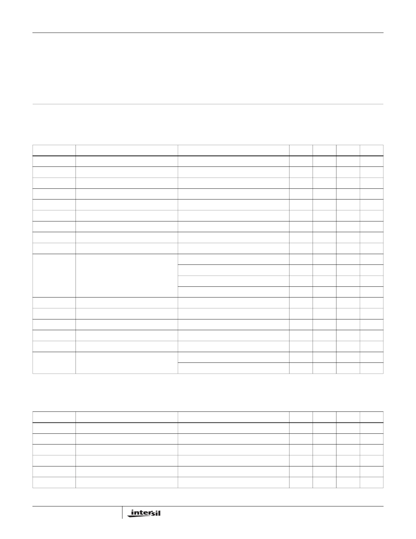
DC Electrical Specifications
V
S
= ±15V, R
L
= 1k
, T
A
= 25°C, unless otherwise specified.
PARAMETER
DESCRIPTION
CONDITION
MIN
TYP
MAX
UNIT
V
OS
Input Offset Voltage
V
S
= ±15V
1.2
5
mV
TCV
OS
Average Offset Voltage Drift
μV/°C
I
B
Input Bias Current
V
S
= ±15V
0.6
3.5
μA
I
OS
Input Offset Current
V
S
= ±15V
0.2
2
μA
TCI
OS
Average Offset Current Drift (Note 1)
TBD
nA/°C
A
VOL
Open-loop Gain
V
S
= ±15V, V
OUT
= ±10V, R
L
= 1k
12000
21000
V/V
PSRR
Power Supply Rejection Ratio
V
S
= ±5V to ±15V
75
100
dB
CMRR
Common-mode Rejection Ratio
V
CM
= ±10V, V
OUT
= 0V
75
90
dB
CMIR
Common-mode Input Range
V
S
= ±15V
13
V
V
OUT
Output Voltage Swing
V
O
+, R
L
= 1k
13.3
13.4
V/V
V
O
-, R
L
= 1k
-12.6
-12.75
V/V
V
O
+, R
L
= 150
9.6
10.7
V/V
V
O
-, R
L
= 150
-6.5
-8.2
V/V
I
SC
Output Short Circuit Current
T
A
= 25°C
80
140
mA
I
S
Supply Current (per amplifier)
V
S
= ±15V, no load
9
9.5
mA
R
IN
Input Resistance
2.0
3.2
M
C
IN
Input Capacitance
A
V
= +1 @10MHz
1
pF
R
OUT
Output Resistance
A
V
= +1
50
m
PSOR
Power Supply Operating Range
Dual supply
±2.25
±15
V
Single supply
4.5
30
V
NOTE:
1. Measured from T
MIN
to T
MAX
.
AC Electrical Specifications
V
S
= ±15V, A
V
= +1, R
L
= 1k
unless otherwise specified.
PARAMETER
DESCRIPTION
CONDITION
MIN
TYP
MAX
UNIT
BW
-3dB Bandwidth (V
OUT
= 0.4V
PP
)
V
S
= ±15V, A
V
= +1
220
MHz
V
S
= ±15V, A
V
= -1
55
MHz
V
S
= ±15V, A
V
= +2
53
MHz
V
S
= ±15V, A
V
= +5
17
MHz
GBWP
Gain Bandwidth Product
V
S
= ±15V
70
MHz
PM
Phase Margin
R
L
= 1k
, C
L
= 5pF
55
°
ISL55002, ISL55004
相关PDF资料 |
PDF描述 |
|---|---|
| ISL55002IB-T13 | High Supply Voltage 220MHz Unity-Gain Stable Operational Amplifiers |
| ISL55002IB-T7 | High Supply Voltage 220MHz Unity-Gain Stable Operational Amplifiers |
| ISL55004IB-T13 | High Supply Voltage 220MHz Unity-Gain Stable Operational Amplifiers |
| ISL55004IB-T7 | High Supply Voltage 220MHz Unity-Gain Stable Operational Amplifiers |
| ISL55013 | MMIC Silicon Bipolar Broadband Amplifier |
相关代理商/技术参数 |
参数描述 |
|---|---|
| ISL55005 | 制造商:INTERSIL 制造商全称:Intersil Corporation 功能描述:MMIC Silicon Bipolar Broadband Amplifier |
| ISL55005 WAF | 制造商:Intersil Corporation 功能描述: |
| ISL55005IEZ | 制造商:Intersil Corporation 功能描述:IC SM AMP RF SILICON BIPOLAR |
| ISL55005IEZ-EVAL | 制造商:Intersil Corporation 功能描述:MMIC SILICON BIPOLAR BROADBAND AMP - Bulk |
| ISL55005IEZ-T7 | 功能描述:IC AMP MMIC BIPO BROADBND SC70-6 RoHS:是 类别:RF/IF 和 RFID >> RF 放大器 系列:- 标准包装:3,000 系列:- 频率:100MHz ~ 6GHz P1dB:9.14dBm(8.2mW) 增益:15.7dB 噪音数据:1.3dB RF 型:CDMA,TDMA,PCS 电源电压:2.7 V ~ 5 V 电流 - 电源:60mA 测试频率:2GHz 封装/外壳:0505(1412 公制) 包装:带卷 (TR) |
发布紧急采购,3分钟左右您将得到回复。