- 您现在的位置:买卖IC网 > PDF目录383135 > ISL55142 (Intersil Corporation) High-Speed 18V CMOS Comparators(高速18V CMOS比较器) PDF资料下载
参数资料
| 型号: | ISL55142 |
| 厂商: | Intersil Corporation |
| 英文描述: | High-Speed 18V CMOS Comparators(高速18V CMOS比较器) |
| 中文描述: | 高速18V的CMOS比较器(高速18V的的CMOS比较器) |
| 文件页数: | 7/14页 |
| 文件大小: | 370K |
| 代理商: | ISL55142 |
7
FN6230.0
July 17, 2006
Power Dissipation Considerations
Specifying continuous data rates, driver loads and driver
level amplitudes are key in determining power supply
requirements as well as dissipation/cooling necessities.
Driver output patterns also impact these needs. The faster
the pin activity, the greater the need to supply current and
remove heat.
The maximum power dissipation allowed in a package is
determined according to:
where:
T
JMAX
= Maximum junction temperature
T
AMAX
= Maximum ambient temperature
θ
JA
= Thermal resistance of the package
P
DMAX
= Maximum power dissipation in the package
Approximate Power Dissipation
(Typ) P = N*[(V
CC
-V
EE
)*8.25mW + 90pF*(V
CC
-V
EE
)^2*f +
CL*(V
OH
-V
OL
)^2*f]
where:
N is the number of comparators in the chip
(1 for ISL55141, 2 for ISL55142 and 4 for ISL55143).
(f) is the operating frequency.
CL is the load capacitor.
The power dissipation calculated from the above formula
may have an error of ±20-25%.
The maximum power dissipation actually produced by an IC
is the total quiescent supply current times the total power
supply voltage, plus the power in the IC due to the loads.
Power also depends on the number of channels changing
state and frequency of operation. The extent of continuous
active pattern generation/reception will greatly affect
dissipation requirements.
The user should evaluate various heat sink/cooling options
in order to control the ambient temperature part of the
equation. This is especially true if the user’s applications
require continuous, high-speed operation.
The reader is cautioned against assuming the same level of
thermal performance in actual applications. A careful
inspection of conditions in your application should be
conducted.
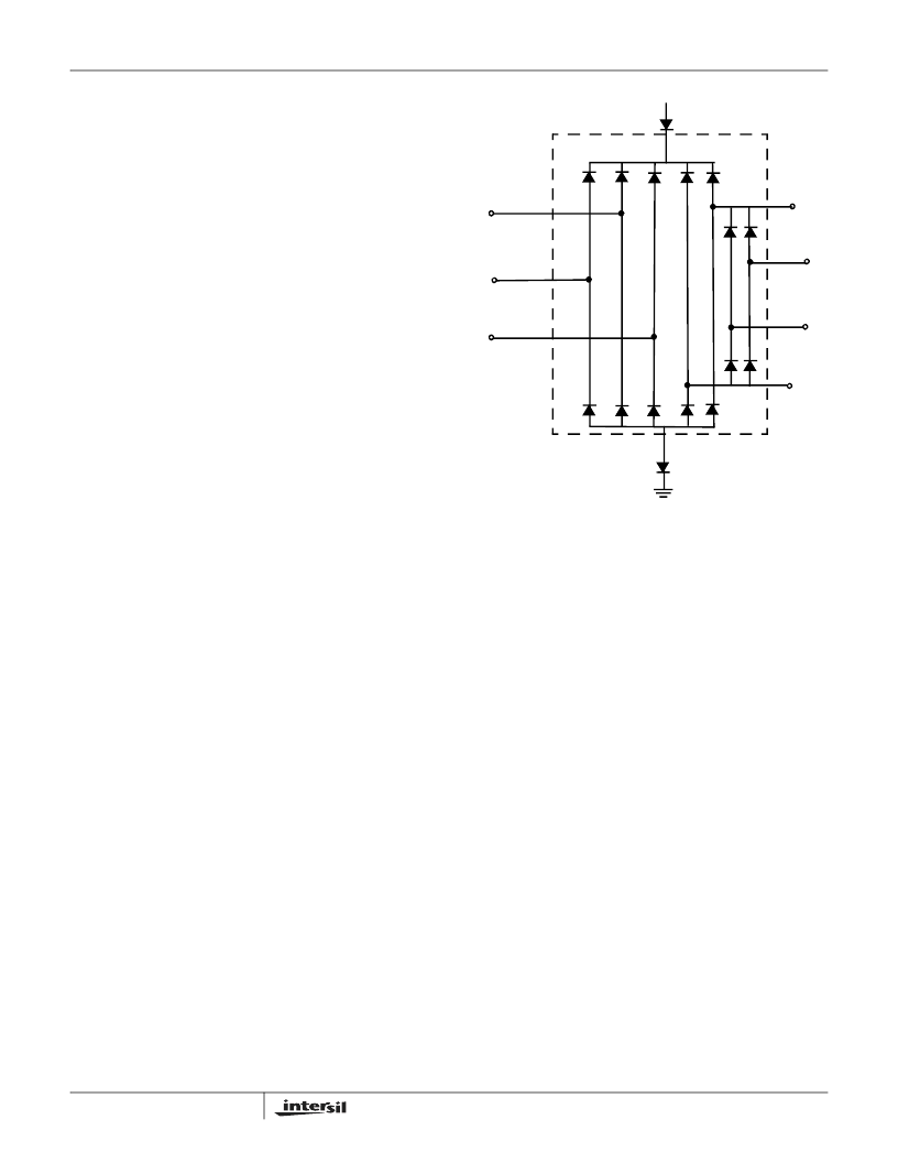
Power Supply Information
Circuit design must always take into account the internal
EOS/ESD protection structure of the device.
Important Note: The QFN package metal plane is used
for heat sinking of the device. It is electrically connected
to the negative supply potential (V
EE
). If V
EE
is tied to
ground, the thermal pad can be connected to ground.
Otherwise, the thermal pad (V
EE
) must be isolated from
other power planes.
Power Supply Sequencing
The ISL55141, ISL55142, ISL55143 reference every supply
with respect to V
EE
. Therefore, apply V
EE
, V
OL
then V
CC
followed by the CV
A
and CV
B
supplies. The comparator
V
INP
pin should not exceed V
EE
or V
CC
during power-up.
In cases where inputs may exceed voltage rails during
power-up, series resistance should be employed to
safeguard EOS to the ESD protection diodes.
P
DMAX
T
- T
JA
--------------------------------------------
=
V
EE
V
OH
V
INP
OPTIONAL PROTECTION
DIODE
V
CC
OPTIONAL PROTECTION
DIODE
Q
A
Q
B
V
OL
CV
A
CV
B
ISL55141, ISL55142, ISL55143
相关PDF资料 |
PDF描述 |
|---|---|
| ISL55141 | High-Speed 18V CMOS Comparators(高速18V CMOS比较器) |
| ISL55143 | High-Speed 18V CMOS Comparators(高速18V CMOS比较器) |
| ISL55191 | Single and Dual Ultra-Low Noise, Ultra-Low Distortion, Rail-to-Rail, Low Power Op Amp |
| ISL55191EVAL1Z | Single and Dual Ultra-Low Noise, Ultra-Low Distortion, Rail-to-Rail, Low Power Op Amp |
| ISL55191IBZ | Single and Dual Ultra-Low Noise, Ultra-Low Distortion, Rail-to-Rail, Low Power Op Amp |
相关代理商/技术参数 |
参数描述 |
|---|---|
| ISL55142IRZ | 功能描述:IC COMP CMOS HS 18V 20-QFN RoHS:是 类别:集成电路 (IC) >> 线性 - 比较器 系列:- 产品培训模块:Lead (SnPb) Finish for COTS Obsolescence Mitigation Program 标准包装:2,500 系列:- 类型:通用 元件数:1 输出类型:CMOS,推挽式,满摆幅,TTL 电压 - 电源,单路/双路(±):2.5 V ~ 5.5 V,±1.25 V ~ 2.75 V 电压 - 输入偏移(最小值):5mV @ 5.5V 电流 - 输入偏压(最小值):1pA @ 5.5V 电流 - 输出(标准):- 电流 - 静态(最大值):24µA CMRR, PSRR(标准):80dB CMRR,80dB PSRR 传输延迟(最大):450ns 磁滞:±3mV 工作温度:-40°C ~ 85°C 封装/外壳:6-WFBGA,CSPBGA 安装类型:表面贴装 包装:管件 其它名称:Q3554586 |
| ISL55142IRZ-T | 功能描述:IC COMP CMOS HS 18V 20-QFN RoHS:是 类别:集成电路 (IC) >> 线性 - 比较器 系列:- 产品培训模块:Lead (SnPb) Finish for COTS Obsolescence Mitigation Program 标准包装:2,500 系列:- 类型:通用 元件数:1 输出类型:CMOS,推挽式,满摆幅,TTL 电压 - 电源,单路/双路(±):2.5 V ~ 5.5 V,±1.25 V ~ 2.75 V 电压 - 输入偏移(最小值):5mV @ 5.5V 电流 - 输入偏压(最小值):1pA @ 5.5V 电流 - 输出(标准):- 电流 - 静态(最大值):24µA CMRR, PSRR(标准):80dB CMRR,80dB PSRR 传输延迟(最大):450ns 磁滞:±3mV 工作温度:-40°C ~ 85°C 封装/外壳:6-WFBGA,CSPBGA 安装类型:表面贴装 包装:管件 其它名称:Q3554586 |
| ISL55142IVZ | 功能描述:IC COMP CMOS HS 18V 20-TSSOP RoHS:是 类别:集成电路 (IC) >> 线性 - 比较器 系列:- 产品培训模块:Lead (SnPb) Finish for COTS Obsolescence Mitigation Program 标准包装:2,500 系列:- 类型:通用 元件数:1 输出类型:CMOS,推挽式,满摆幅,TTL 电压 - 电源,单路/双路(±):2.5 V ~ 5.5 V,±1.25 V ~ 2.75 V 电压 - 输入偏移(最小值):5mV @ 5.5V 电流 - 输入偏压(最小值):1pA @ 5.5V 电流 - 输出(标准):- 电流 - 静态(最大值):24µA CMRR, PSRR(标准):80dB CMRR,80dB PSRR 传输延迟(最大):450ns 磁滞:±3mV 工作温度:-40°C ~ 85°C 封装/外壳:6-WFBGA,CSPBGA 安装类型:表面贴装 包装:管件 其它名称:Q3554586 |
| ISL55142IVZEVAL1Z | 功能描述:EVALUATION BOARD FOR ISL55142IVZ RoHS:是 类别:编程器,开发系统 >> 评估演示板和套件 系列:* 标准包装:1 系列:PCI Express® (PCIe) 主要目的:接口,收发器,PCI Express 嵌入式:- 已用 IC / 零件:DS80PCI800 主要属性:- 次要属性:- 已供物品:板 |
| ISL55142IVZ-T | 功能描述:IC COMP CMOS HS 18V 20-TSSOP RoHS:是 类别:集成电路 (IC) >> 线性 - 比较器 系列:- 产品培训模块:Lead (SnPb) Finish for COTS Obsolescence Mitigation Program 标准包装:2,500 系列:- 类型:通用 元件数:1 输出类型:CMOS,推挽式,满摆幅,TTL 电压 - 电源,单路/双路(±):2.5 V ~ 5.5 V,±1.25 V ~ 2.75 V 电压 - 输入偏移(最小值):5mV @ 5.5V 电流 - 输入偏压(最小值):1pA @ 5.5V 电流 - 输出(标准):- 电流 - 静态(最大值):24µA CMRR, PSRR(标准):80dB CMRR,80dB PSRR 传输延迟(最大):450ns 磁滞:±3mV 工作温度:-40°C ~ 85°C 封装/外壳:6-WFBGA,CSPBGA 安装类型:表面贴装 包装:管件 其它名称:Q3554586 |
发布紧急采购,3分钟左右您将得到回复。