- 您现在的位置:买卖IC网 > PDF目录383137 > ISL59424IR-T7 (INTERSIL CORP) 1GHz Triple Multiplexing Amplifiers PDF资料下载
参数资料
| 型号: | ISL59424IR-T7 |
| 厂商: | INTERSIL CORP |
| 元件分类: | 运动控制电子 |
| 英文描述: | 1GHz Triple Multiplexing Amplifiers |
| 中文描述: | TRIPLE 2-CHANNEL, VIDEO MULTIPLEXER, QCC24 |
| 封装: | QFN-24 |
| 文件页数: | 8/13页 |
| 文件大小: | 780K |
| 代理商: | ISL59424IR-T7 |
8
FN7456.2
September 8, 2005
Pin Descriptions
ISL59445
(32-PIN QFN)
ISL59424
(24-PIN QFN)
PIN
NAME
EQUIVALENT
CIRCUIT
DESCRIPTION
1
5
IN1A
Circuit 1.
Channel 1 input for output amplifier "A"
2, 4, 8, 13, 15,
24, 28, 30
2, 8, 10, 11,
21, 22
NIC
N
ot
I
nternally
C
onnected; it is recommended these pins be tied to ground to
minimize crosstalk.
3
7
IN1B
Circuit 1.
Channel 1 input for output amplifier "B"
5
9
IN1C
Circuit 1.
Channel 1 input for output amplifier "C"
6
4
GNDB
Circuit 4.
Ground pin for output amplifier “B”
7
IN2A
Circuit 1.
Channel 2 input for output amplifier "A"
9
IN2B
Circuit 1.
Channel 2 input for output amplifier "B"
10
IN2C
Circuit 1.
Channel 2 input for output amplifier "C"
11
6
GNDC
Circuit 4.
Ground pin for output amplifier “C”
12
IN3A
Circuit 1.
Channel 3 input for output amplifier "A"
14
IN3B
Circuit 1.
Channel 3 input for output amplifier "B"
16
IN3C
Circuit 1.
Channel 3 input for output amplifier "C"
17
S1
Circuit 2.
Channel selection pin MSB (binary logic code)
18
13
S0
Circuit 2.
Channel selection pin. LSB (binary logic code)
19
14
OUTC
Circuit 3.
Output of amplifier “C”
20
16
OUTB
Circuit 3.
Output of amplifier “B”
21
15
V-
Circuit 4.
Negative power supply
22
18
OUTA
Circuit 3.
Output of amplifier “A”
23
17
V+
Circuit 4.
Positive power supply
25
19
ENABLE
Circuit 2.
Device enable (active low). Internal pull-down resistor ensures the device will be
active with no connection to this pin. A logic High on this pin puts device into power-
down mode. In power-down mode only logic circuitry is active. All logic states are
preserved post power-down. This state is not recommended for logic control where
more than one MUX-amp share the same video output line.
12
LE
Circuit 2.
Device latch enable on the ISL59424. A logic high on LE will latch the last (S0, S1)
logic state. HIZ and ENABLE functions are not latched with the LE pin.
26
20
HIZ
Circuit 2.
Output disable (active high). Internal pull-down resistor ensures the device will be
active with no connection to this pin. A logic high, puts the outputs in a high
impedance state. Use this state to control logic when more than one MUX-amp
share the same video output line.
27
3
IN0C
Circuit 1.
Channel 0 for output amplifier "C"
29
1
IN0B
Circuit 1.
Channel 0 for output amplifier "B"
31
23
IN0A
Circuit 1.
Channel 0 for output amplifier "A"
32
24
GNDA
Circuit 4.
Ground pin for output amplifier “A”
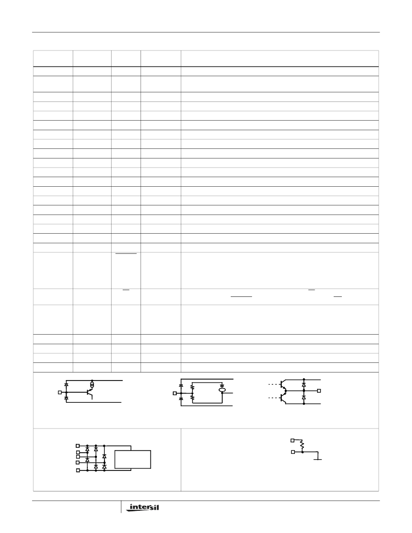
IN
V+
V-
LOGIC PIN
V+
V-
GND.
33K
21K
+
-
1.2V
V+
V-
OUT
CIRCUIT 3
CIRCUIT 1
CIRCUIT 2
V-
V+
GNDA
GNDB
GNDC
CAPACITIVELY
COUPLED
ESD CLAMP
CIRCUIT 4
V-
THERMAL HEAT SINK PAD
~1M
SUBSTRATE
ISL59424, ISL59445
.
相关PDF资料 |
PDF描述 |
|---|---|
| ISL59424 | 1GHz Triple Multiplexing Amplifiers |
| ISL59424IR | 1GHz Triple Multiplexing Amplifiers |
| ISL59424IRZ | 1GHz Triple Multiplexing Amplifiers |
| ISL59424IRZ-T13 | 1GHz Triple Multiplexing Amplifiers |
| ISL59424IRZ-T7 | 1GHz Triple Multiplexing Amplifiers |
相关代理商/技术参数 |
参数描述 |
|---|---|
| ISL59424IRZ | 制造商:Intersil Corporation 功能描述:ANLG MUX/AMP TRIPLE 2:1 24QFN EP - Bulk 制造商:Intersil Corporation 功能描述:1GHz Triple Multiplexing Amplifiers |
| ISL59424IRZ-T13 | 制造商:Intersil Corporation 功能描述:ANLG MUX/AMP TRIPLE 2:1 24QFN EP - Tape and Reel |
| ISL59424IRZ-T7 | 制造商:Intersil Corporation 功能描述:ANLG MUX/AMP TRIPLE 2:1 24QFN EP - Tape and Reel 制造商:Intersil 功能描述:Intersil ISL59424IRZ-T7 Analog Switch Multiplexers 制造商:Intersil 功能描述:ISL80102 EVAL 2 10LD 2A BAG&SHIP IC DIFER |
| ISL59440 | 制造商:INTERSIL 制造商全称:Intersil Corporation 功能描述:400MHz Multiplexing Amplifier |
| ISL59440_07 | 制造商:INTERSIL 制造商全称:Intersil Corporation 功能描述:400MHz Multiplexing Amplifier |
发布紧急采购,3分钟左右您将得到回复。