参数资料
| 型号: | ISL59532IKEZ |
| 厂商: | Intersil |
| 文件页数: | 15/25页 |
| 文件大小: | 0K |
| 描述: | IC CROSSPOINT SW 32X32 356BGA |
| 标准包装: | 40 |
| 功能: | 视频交叉点开关 |
| 电路: | 1 x 32:32 |
| 电压电源: | 单电源 |
| 电压 - 电源,单路/双路(±): | 4.5 V ~ 5.5 V |
| 电流 - 电源: | 640mA |
| 工作温度: | -40°C ~ 85°C |
| 安装类型: | 表面贴装 |
| 封装/外壳: | 356-BBGA 裸露焊盘 |
| 供应商设备封装: | 356-HPBGA(27x27) |
| 包装: | 托盘 |
| 产品目录页面: | 1247 (CN2011-ZH PDF) |
22
FN7432.7
October 26, 2011
For this reason, the ISL59532 must be in DC-coupled
mode (Clamp Disabled) to be compatible with s-video
and component video signals.
Bandwidth Considerations
Wide frequency response (high bandwidth) in a video
system means better video resolution. Four sets of
frequency response curves are shown in Figure 47.
Depending on the switch configurations, and the routing (the
path from the input to the output), bandwidth can vary
between 100MHz and 350MHz. A short discussion of the
trade-offs — including matrix configuration, output buffer
gain selection, channel selection, and loading — follows.
In multiplexer mode, one input typically drives one output
channel, while in broadcast mode, one input drives all 32
outputs. As the number of outputs driven increases, the
parasitic loading on that input increases. Broadcast Mode is
the worst-case, where the capacitance of all 32 channels
loads one input, reducing the overall bandwidth. In addition,
due to internal device compensation, an output buffer gain of
x2 has higher bandwidth than a gain of x1. Therefore, the
highest bandwidth configuration is multiplexer mode (with
each input mapped to only one output) and an output buffer
gain of x2.
The relative locations of the input and output channels also
have significant impact on the device bandwidth (due to the
layout of the ISL59530 silicon). When the input and output
channels are further away, there are additional parasitics as
a result of the additional routing, resulting in lower
bandwidth.
The bandwidth does not change significantly with resistive
loading as shown in the typical performance curves.
However several of the curves demonstrate that frequency
response is sensitive to capacitance loading. This is most
significant when laying out the PCB. If the PCB trace length
between the output of the crosspoint switch and the back-
termination resistor is not minimized, the additional parasitic
capacitance will result in some peaking and eventually a
reduction in overall bandwidth.
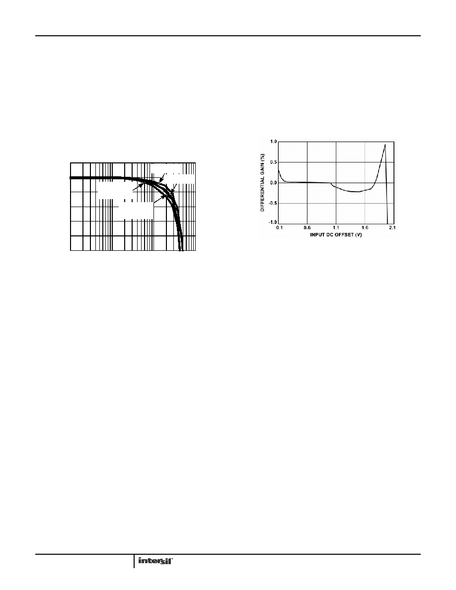
Linear Operating Region
In addition to bandwidth optimization, to get the best linearity
the ISL59532 should be configured to operate in its most
linear operating region. Figure 48 shows the differential gain
curve. The ISL59532 is a single supply 5V design with its
most linear region between 0.1 and 2V. This range is fine for
most video signals whose nominal signal amplitude is 1V.
The most negative input level (the sync tip for composite
video) should be maintained at 0.3V or above for best
operation.
In a DC-coupled application, it is the system designer’s
responsibility to ensure that the video signal is always in the
optimum range.
When AC coupling, the ISL59532’s Clamp (also called “DC
restore”) function automatically and continuously adjusts the
DC level so that the most negative portion of the video is
always equal to VREF.
A discussion of the benefits of the DC restoration function
begins by understanding the Clamp circuit shown in
Figure 49. The incoming video signal is typically terminated
into 75
Ω, then AC coupled through C1, at which point it is
connected to the base of the buffer’s diff pair. These
components form the video path.
The Clamp function consists of Q1, D1, Q2, D2, the two
current sources, and the 3 switches controlled by the Clamp
Enable signal. The VREF voltage is level-shifted up two
diode drops (Q1 and D1) to the base of Q2. If the voltage at
the cathode of D2 goes below VREF, Q2 and D2 will turn on,
keeping the INx voltage at VREF. If the voltage at INx is
greater than VREF, Q2 and D2 are off and the INx node is
high impedance. This is how the clamp function forces the
lowest portion of the video signal (the sync tip) to always be
equal to or greater than VREF.
To make sure that the sync tip is always equal to (not equal
to or greater than) VREF, i1 is constantly sinking ~2A of
current from C1. This causes each sync tip to be slightly
lower voltage than the previous sync tip, causing Q2 and D2
to turn on at each sync tip and raise the voltage to VREF. The
2A pull-down with a 0.1uF capacitor and a 15kHz HSYNC
frequency results in 1.3mV of “droop” across every line, or
FIGURE 47. FREQUENCY RESPONSE FOR VARIOUS MODES
FREQUENCY (MHz)
NORMALIZ
E
D
GAIN
(dB)
MUX, AV = 2
BROADCAST,
AV = 1
BROADCAST,
AV = 2
MUX, AV = 1
-10
-8
-6
-4
-2
0
2
-10
-8
-6
-4
-2
0
2
1
10
100
1000
FIGURE 48. DIFFERENTIAL GAIN RESPONSE
ISL59532
相关PDF资料 |
PDF描述 |
|---|---|
| ISL59534IKEZ | IC CROSSPOINT SW 32X16 356BGA |
| ISL6436LIB | IC CTRLR PS USB DUAL PORT 8-SOIC |
| ISL76120ARTZ-T | IC MULTIPLEXER DUAL SPDT 10TDFN |
| ISL76321ARZ | IC VIDEO SERDES LONG 16BIT 48QFN |
| ISL76322ARZ | IC VIDEO SERDES LONG 16BIT 48QFN |
相关代理商/技术参数 |
参数描述 |
|---|---|
| ISL59533 | 制造商:INTERSIL 制造商全称:Intersil Corporation 功能描述:32x32 Video Crosspoint with Differential Inputs |
| ISL59533IKEZ | 制造商:INTERSIL 制造商全称:Intersil Corporation 功能描述:32x32 Video Crosspoint with Differential Inputs |
| ISL59534 | 制造商:INTERSIL 制造商全称:Intersil Corporation 功能描述:32x16 Video Crosspoint |
| ISL59534_0708 | 制造商:INTERSIL 制造商全称:Intersil Corporation 功能描述:32x16 Video Crosspoint |
| ISL59534IKEZ | 功能描述:IC CROSSPOINT SW 32X16 356BGA RoHS:是 类别:集成电路 (IC) >> 接口 - 模拟开关,多路复用器,多路分解器 系列:- 应用说明:Ultrasound Imaging Systems Application Note 产品培训模块:Lead (SnPb) Finish for COTS Obsolescence Mitigation Program 标准包装:250 系列:- 功能:开关 电路:单刀单掷 导通状态电阻:48 欧姆 电压电源:单电源 电压 - 电源,单路/双路(±):2.7 V ~ 5.5 V 电流 - 电源:5µA 工作温度:0°C ~ 70°C 安装类型:表面贴装 封装/外壳:48-LQFP 供应商设备封装:48-LQFP(7x7) 包装:托盘 |
发布紧急采购,3分钟左右您将得到回复。