- 您现在的位置:买卖IC网 > PDF目录10521 > ISL59913IRZ (Intersil)IC RCVR/EQUALZR TRPL DIFF 28-QFN PDF资料下载
参数资料
| 型号: | ISL59913IRZ |
| 厂商: | Intersil |
| 文件页数: | 12/12页 |
| 文件大小: | 0K |
| 描述: | IC RCVR/EQUALZR TRPL DIFF 28-QFN |
| 标准包装: | 90 |
| 类型: | 接收器 |
| 驱动器/接收器数: | 0/3 |
| 规程: | 双绞线 |
| 电源电压: | 5V |
| 安装类型: | 表面贴装 |
| 封装/外壳: | 28-VFQFN 裸露焊盘 |
| 供应商设备封装: | 28-QFN(4x5) |
| 包装: | 管件 |
| 产品目录页面: | 1241 (CN2011-ZH PDF) |
9
FN6406.0
December 15, 2006
Applications Information
Logic Control
The ISL59913 has two logical input pins, Chip Enable
(ENABLE) and Switch Gain (X2). The logic circuits all have a
nominal threshold of 1.1V above the potential of the logic
reference pin (VREF). In most applications it is expected that
this chip will run from a +5V, 0V, -5V supply system with logic
being run between 0V and +5V. In this case the logic
reference voltage should be tied to the 0V supply. If the logic
is referenced to the -5V rail, then the logic reference should
be connected to -5V. The logic reference pin sources about
60A and this will rise to about 200A if all inputs are true
(positive).
The logic inputs all source up to 10A when they are held at
the logic reference level. When taken positive, the inputs
sink a current dependent on the high level, up to 50A for a
high level 5V above the reference level.
The logic inputs, if not used, should be tied to the
appropriate voltage in order to define their state.
Control Reference and Signal Reference
Analog control voltages are required to set the equalizer and
contrast levels. These signals are voltages in the range
0V to 1V, which are referenced to the control reference pin. It
is expected that the control reference pin will be tied to 0V
and the control voltage will vary from 0V to 1V. It is; however,
acceptable to connect the control reference to any potential
between -5V and 0V to which the control voltages are
referenced.
The control voltage pins themselves are high impedance.
The control reference pin will source between 0A and
200A depending on the control voltages being applied.
The control reference and logic reference effectively remove
the necessity for the 0V rail and operation from ±5V (or 0V
and 10V) only is possible. However we still need a further
reference to define the 0V level of the single ended output
signal. The reference for the output signal is provided by the
0V pin. The output stage cannot pull fully up or down to either
supply so it is important that the reference is positioned to
allow full output swing. The 0V reference should be tied to a
'quiet ground' as any noise on this pin is transferred directly to
the output. The 0V pin is a high impedance pin and draws DC
bias currents of a few A and similar levels of AC current.
Equalizing
When transmitting a signal across a twisted pair cable, it is
found that the high frequency (above 1MHz) information is
attenuated more significantly than the information at low
frequencies. The attenuation is predominantly due to resistive
skin effect losses and has a loss curve which depends on the
resistivity of the conductor, surface condition of the wire and the
wire diameter. For the range of high performance twisted pair
cables based on 24awg copper wire (CAT-5 etc). These
parameters vary only a little between cable types and in general
cables exhibit the same frequency dependence of loss. (The
lower loss cables can be compared with somewhat longer
lengths of their more lossy brothers.) This enables a single
equalizing law equation to be built into the ISL59913.
With a control voltage applied between pins VCTRL and
VREF, the frequency dependence of the equalization is
shown in Figure 8. The equalization matches the cable loss
up to about 100MHz. Above this, system gain is rolled off
rapidly to reduce noise bandwidth. The roll-off occurs more
rapidly for higher control voltages, thus the system (cable +
equalizer) bandwidth reduces as the cable length increases.
This is desirable, as noise becomes an increasing issue as
the equalization increases.
Typical Performance Curves (Continued)
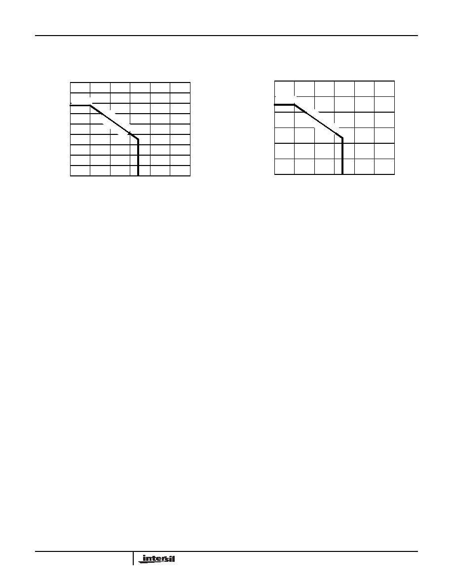
FIGURE 23. PACKAGE POWER DISSIPATION vs AMBIENT
TEMPERATURE
FIGURE 24. PACKAGE POWER DISSIPATION vs AMBIENT
TEMPERATURE
JEDEC JESD51-7 HIGH EFFECTIVE THERMAL
CONDUCTIVITY TEST BOARD - QFN EXPOSED
DIEPAD SOLDERED TO PCB PER JESD51-5
θ
JA =
37
°C
/W
QF
N2
8
3.378W
0
50
85
150
4.5
3.5
2.5
1.5
0.5
0
AMBIENT TEMPERATURE (°C)
POW
E
R
DISS
IP
A
T
ION
(W)
25
75
100
125
4
2
1
3
JEDEC JESD51-3 LOW EFFECTIVE THERMAL
CONDUCTIVITY TEST BOARD
893mW
θ
JA =
14
0°C
/W
QF
N2
8
0
50
85
150
1.2
0.8
0.6
0.4
0.2
0
AMBIENT TEMPERATURE (°C)
POWE
R
DI
SSI
P
A
TI
ON
(W)
25
75
100
125
1
ISL59910, ISL59913
相关PDF资料 |
PDF描述 |
|---|---|
| VE-2TM-IW-F2 | CONVERTER MOD DC/DC 10V 100W |
| MS3102A22-18S | CONN RCPT 8POS BOX MNT W/SCKT |
| MS3101A18-4P | CONN RCPT 4POS FREE HNG W/PINS |
| LTC2248CUH#PBF | IC ADC 14-BIT 65MSPS 3V 32-QFN |
| VI-J4Z-MX-F4 | CONVERTER MOD DC/DC 2V 30W |
相关代理商/技术参数 |
参数描述 |
|---|---|
| ISL59913IRZ-EVALZ | 功能描述:EVAL BOARD FOR ISL59913IRZ RoHS:是 类别:编程器,开发系统 >> 评估演示板和套件 系列:* 标准包装:1 系列:PCI Express® (PCIe) 主要目的:接口,收发器,PCI Express 嵌入式:- 已用 IC / 零件:DS80PCI800 主要属性:- 次要属性:- 已供物品:板 |
| ISL59913IRZ-T7 | 功能描述:视频 IC ISL95210 5V/10AUCK FET INDSTRL TEMP RNG RoHS:否 制造商:Fairchild Semiconductor 工作电源电压:5 V 电源电流:80 mA 最大工作温度:+ 85 C 封装 / 箱体:TSSOP-28 封装:Reel |
| ISL59920 | 制造商:INTERSIL 制造商全称:Intersil Corporation 功能描述:Triple Analog Video Delay Lines |
| ISL59920_09 | 制造商:INTERSIL 制造商全称:Intersil Corporation 功能描述:Triple Analog Video Delay Lines |
| ISL59920IRZ | 功能描述:视频 IC ISL95311W I2C 128POS POS DCP 10KOHM S+/-5 RoHS:否 制造商:Fairchild Semiconductor 工作电源电压:5 V 电源电流:80 mA 最大工作温度:+ 85 C 封装 / 箱体:TSSOP-28 封装:Reel |
发布紧急采购,3分钟左右您将得到回复。