- 您现在的位置:买卖IC网 > PDF目录383139 > ISL60007DIB825 (INTERSIL CORP) GT 14C 14#16 SKT RECP BOX PDF资料下载
参数资料
| 型号: | ISL60007DIB825 |
| 厂商: | INTERSIL CORP |
| 元件分类: | 基准电压源/电流源 |
| 英文描述: | GT 14C 14#16 SKT RECP BOX |
| 中文描述: | 1-OUTPUT THREE TERM VOLTAGE REFERENCE, 2.5 V, PDSO8 |
| 封装: | SOIC-8 |
| 文件页数: | 8/12页 |
| 文件大小: | 469K |
| 代理商: | ISL60007DIB825 |
8
FN8087.1
May 5, 2005
Applications Information
FGA Technology
The ISL60007 series of voltage references use the floating
gate technology to create references with very low drift and
supply current. Essentially the charge stored on a floating
gate cell is set precisely in manufacturing. The reference
voltage output itself is a buffered version of the floating gate
voltage. The resulting reference device has excellent
characteristics which are unique in the industry: very low
temperature drift, high initial accuracy, and almost zero
supply current. Also, the reference voltage itself is not limited
by voltage bandgaps or zener settings, so a wide range of
reference voltages can be programmed (standard voltage
settings are provided, but customer-specific voltages are
available).
The process used for these reference devices is a floating
gate CMOS process, and the amplifier circuitry uses CMOS
transistors for amplifier and output transistor circuitry. While
providing excellent accuracy, there are limitations in output
noise level and load regulation due to the MOS device
characteristics. These limitations are addressed with circuit
techniques discussed in other sections.
Nanopower Operation
Reference devices achieve their highest accuracy when
powered up continuously, and after initial stabilization has
taken place. This drift can be eliminated by leaving the
power on continuously.
The ISL60007 is the first high precision voltage reference
with ultra low power consumption that makes it possible to
leave power on continuously in battery operated circuits. The
ISL60007 consumes extremely low supply current due to the
proprietary FGA technology. Supply current at room
temperature is typically 400nA which is 1 to 2 orders of
magnitude lower than competitive devices. Application
circuits using battery power will benefit greatly from having
an accurate, stable reference which essentially presents no
load to the battery.
In particular, battery powered data converter circuits that
would normally require the entire circuit to be disabled when
not in use can remain powered up between conversions as
shown in Figure 27. Data acquisition circuits providing 12 to
24 bits of accuracy can operate with the reference device
continuously biased with no power penalty, providing the
highest accuracy and lowest possible long term drift.
Other reference devices consuming higher supply currents
will need to be disabled in between conversions to conserve
battery capacity. Absolute accuracy will suffer as the device
is biased and requires time to settle to its final value, or, may
not actually settle to a final value as power on time may be
short.
Board Mounting Considerations
For applications requiring the highest accuracy, board
mounting location should be reviewed. Placing the device in
areas subject to slight twisting can cause degradation of the
accuracy of the reference voltage due to die stresses. It is
normally best to place the device near the edge of a board,
or the shortest side, as the axis of bending is most limited at
that location. Obviously mounting the device on flexprint or
extremely thin PC material will likewise cause loss of
reference accuracy.
Noise Performance and Reduction
The output noise voltage in a 0.1Hz to 10Hz bandwidth is
typically 30μV
P-P
. This is shown in the plot in the Typical
Performance Curves. The noise measurement is made with
a bandpass filter made of a 1 pole high-pass filter with a
corner frequency at 0.1Hz and a 2-pole low-pass filter with a
corner frequency at 12.6Hz to create a filter with a 9.9Hz
bandwidth. Noise in the 10kHz to 1MHz bandwidth is
approximately 400μV
P-P
with no capacitance on the output,
as shown in Figure 28. These noise measurements are
made with a 2 decade bandpass filter made of a 1 pole high-
pass filter with a corner frequency at 1/10 of the center
frequency and 1-pole low-pass filter with a corner frequency
at 10 times the center frequency. Figure 28 also shows the
noise in the 10kHz to 1MHz band can be reduced to about
50μV
P-P
using a 0.001μF capacitor on the output. Noise in
the 1kHz to 100kHz band can be further reduced using a
0.1μF capacitor on the output, but noise in the 1Hz to 100Hz
band increases due to instability of the very low power
amplifier with a 0.1μF capacitance load. For load
capacitances above 0.001μF the noise reduction network
shown in Figure 29 is recommended. This network reduces
noise significantly over the full bandwidth. As shown in
Figure 28, noise is reduced to less than 40μV
P-P
from 1Hz
to 1MHz using this network with a 0.01μF capacitor and a
2k
resistor in series with a 10μF capacitor.
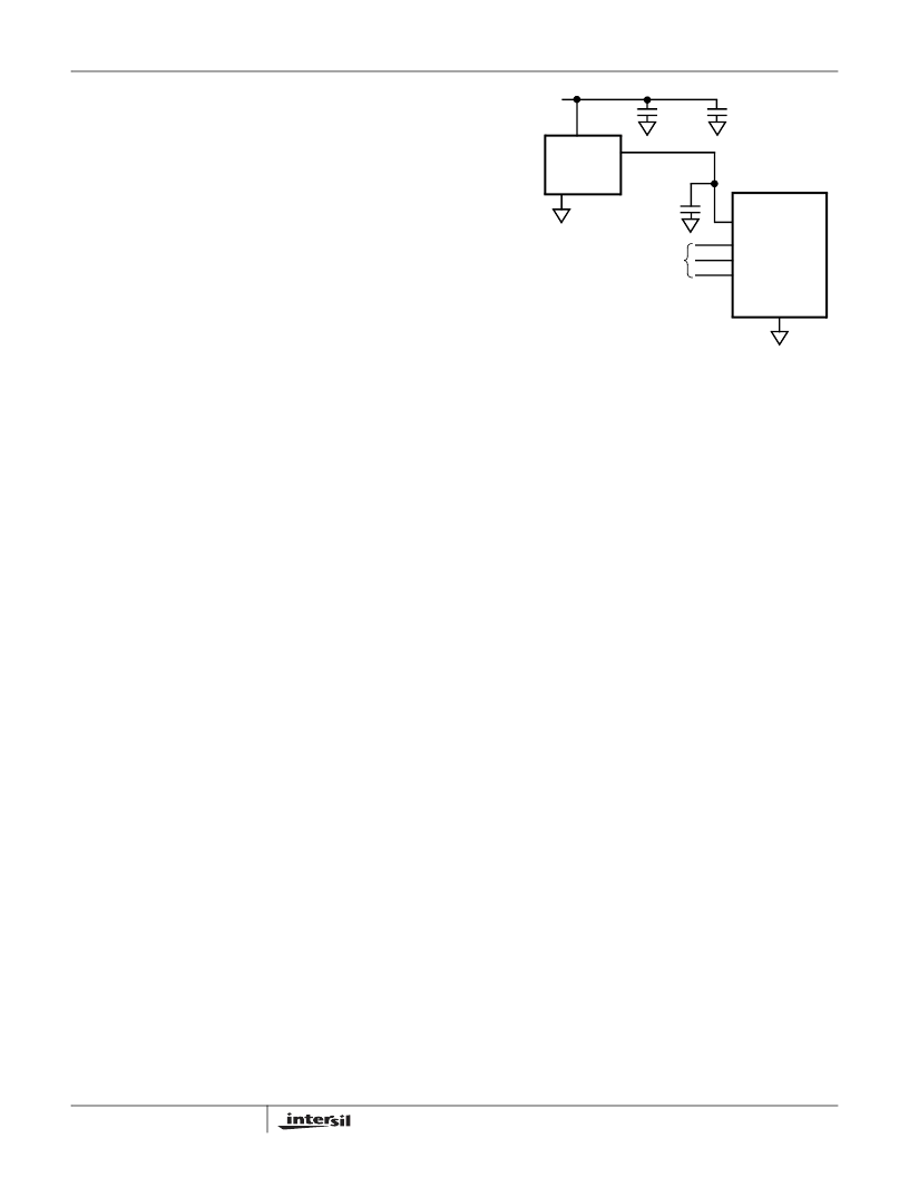
V
IN
= +3.0V
0.001μF-0.01μF
SERIAL
BUS
V
IN
V
OUT
ISL60007
GND
REF IN
ENABLE
SCK
SDAT
12 TO 24-BIT
A/D CONVERTER
0.01μF
10μF
FIGURE 27.
ISL60007
相关PDF资料 |
PDF描述 |
|---|---|
| ISL60007CIB812 | Precision 1.25V and 2.50V, 1.08?-Watt, High Precision FGA Voltage References |
| ISL60007DIB812 | Precision 1.25V and 2.50V, 1.08?-Watt, High Precision FGA Voltage References |
| ISL6111 | Current Regulated PCI Hot Plug Power Switch Controller |
| ISL6111CRZA | Current Regulated PCI Hot Plug Power Switch Controller |
| ISL6111EVAL2 | Current Regulated PCI Hot Plug Power Switch Controller |
相关代理商/技术参数 |
参数描述 |
|---|---|
| ISL60007DIB825-TK | 功能描述:IC VREF SERIES PREC 2.5V 8-SOIC RoHS:否 类别:集成电路 (IC) >> PMIC - 电压基准 系列:FGA™ 标准包装:3,000 系列:- 基准类型:旁路,精度 输出电压:5V 容差:±0.5% 温度系数:100ppm/°C 输入电压:- 通道数:1 电流 - 阴极:80µA 电流 - 静态:- 电流 - 输出:15mA 工作温度:-40°C ~ 85°C 安装类型:表面贴装 封装/外壳:TO-236-3,SC-59,SOT-23-3 供应商设备封装:SOT-23-3 包装:带卷 (TR) 其它名称:LM4040CIM3-5.0MLTRLM4040CIM3-5.0MLTR-ND |
| ISL60007DIB825Z | 制造商:INTERSIL 制造商全称:Intersil Corporation 功能描述:Precision 2.50V, 1.08U-Watt, High Precision FGA Voltage References |
| ISL60008-50AZ6 WAF | 制造商:Intersil Corporation 功能描述: |
| ISL6111 | 制造商:INTERSIL 制造商全称:Intersil Corporation 功能描述:Current Regulated PCI Hot Plug Power Switch Controller |
| ISL6111CR | 功能描述:IC CTRLR HOT PLUG SWITCH 20-QFN RoHS:否 类别:集成电路 (IC) >> PMIC - 热交换 系列:- 产品培训模块:Obsolescence Mitigation Program 标准包装:100 系列:- 类型:热插拔开关 应用:通用 内部开关:是 电流限制:可调 电源电压:9 V ~ 13.2 V 工作温度:-40°C ~ 150°C 安装类型:表面贴装 封装/外壳:10-WFDFN 裸露焊盘 供应商设备封装:10-TDFN-EP(3x3) 包装:管件 |
发布紧急采购,3分钟左右您将得到回复。