- 您现在的位置:买卖IC网 > PDF目录20083 > ISL6161CBZA-T (Intersil)IC CTLR PWR DISTRIB DUAL 14SOIC PDF资料下载
参数资料
| 型号: | ISL6161CBZA-T |
| 厂商: | Intersil |
| 文件页数: | 6/11页 |
| 文件大小: | 215K |
| 描述: | IC CTLR PWR DISTRIB DUAL 14SOIC |
| 标准包装: | 1 |
| 类型: | 热交换控制器 |
| 应用: | 通用型,PCI Express? |
| 内部开关: | 无 |
| 电源电压: | 10.5 V ~ 13.2 V |
| 工作温度: | 0°C ~ 70°C |
| 安装类型: | 表面贴装 |
| 封装/外壳: | 14-SOIC(0.154",3.90mm 宽) |
| 供应商设备封装: | 14-SOICN |
| 包装: | 标准包装 |
| 产品目录页面: | 1244 (CN2011-ZH PDF) |
| 其它名称: | ISL6161CBZA-TDKR |
6
FN9104.4
October 2, 2008
.
The ISL6161 responds to a load short (defined as a current
level 3x the OC set point with a fast transition) by
immediately driving the relevant N-Channel MOSFET gate to
0V in ~3祍. The gate voltage is then slowly ramped up,
soft-starting the N-Channel MOSFET to the programmed
current regulation limit level. This is the start of the time-out
period if the abnormal load condition still exists. The
programmed current regulation level is held until either the
OC event passes or the time-out period expires. If the former
is the case, then the N-Channel MOSFET is fully enhanced
and the C
TIM
charging current is diverted away from the
capacitor. If the time-out period expires prior to OC
resolution, then both gates are quickly pulled to 0V turning
off both N-Channel MOSFETs simultaneously.
Upon any UV condition, the PGOOD signal will pull low
when tied high through a resistor to the logic supply. This pin
is a fault indicator but not the OC latch-off indicator. For an
OC latch-off indication, monitor CTIM, pin 10. This pin will
rise rapidly to 12V once the time-out period expires. See
Simplified Schematic
on page 2 for OC latch-off circuit
suggestion.
The ISL6161 is reset by a rising edge on the ENABLE
pin
and is turned on by the ENABLE
pin being driven low.
ISL6161 Application Considerations
In a non PCI-Express, motor drive application, Current loop
stabilization is facilitated through a small value resistor in
series with the gate timing capacitor. As the ISL6161 drives
a highly inductive current load, instability characterized by
the gate voltage repeatedly ramping up and down may
appear. A simple method to enhance stability is provided by
the substitution of a larger value gate resistor. Typically, this
situation can be avoided by eliminating long point-to-point
wiring to the load.
With the ENABLE internal pull-up, the ISL6161 is well suited
for implementation on either side of the connector where a
motherboard prebiased condition or a load board staggered
connection is present. In either case, the ISL6161 turns on in
a soft-start mode protecting the supply rail from sudden
current loading.
During the Time-Out delay period with the ISL6161 in
current limit mode, the V
GS
of the external N-Channel
MOSFETs is reduced driving the N-Channel MOSFET switch
into a high r
DS(ON)
state. Thus, avoid extended time-out
periods as the external N-Channel MOSFETs may be
damaged or destroyed due to excessive internal power
dissipation. Refer to the MOSFET manufacturers data sheet
for SOA information.
With the high levels of in-rush current e.g., highly capacitive
loads and motor start-up currents, choosing the current
regulation (CR) level is crucial to provide both protection
and still allow for this in-rush current without latching off.
Consider this in addition to the time-out delay when
choosing MOSFETs for your design.
Physical layout of R
SENSE
resistors is critical to avoid
inadvertently lowering the CR and trip levels. Ideally, trace
routing between the R
SENSE
resistors and the ISL6161
should be as direct and as short as possible with zero
current in the sense lines.
TABLE 1. R
SENSE
AND R
ILIM
RECOMMENDATIONS
PCI-EXPRESS
ADD-IN CARD
CONNECTOR
R
ILIM
(k?/SPAN>)
3.3V R
SENSE
(m?/SPAN>),
NOMINAL
CR (A)
12V R
SENSE
(m?/SPAN>),
NOMINAL
CR (A)
NOMINAL
CRVth
(mV)
X1
10
30, 3.3
150, 0.7
100
4.99
15, 3.5
90, 0.6
53
X4/X8
10
30, 3.3
40, 2.5
100
4.99
15, 3.5
20, 2.6
53
X16
10
30, 3.3
16, 6.3
100
4.99
15, 3.5
8, 6.6
53
NOTE: Nominal CR Vth = R
ILIM
x 10礎.
TABLE 2.
C
TIM
CAPACITOR
(礔)
NOMINAL TIME-OUT PERIOD
(ms)
0.022
4.4
0.047
9.4
0.1
20
NOTE: Nominal time-out period in seconds = C
TIM
x 200k?
CORRECT
TO ISEN AND
CURRENT
SENSE RESISTOR
INCORRECT
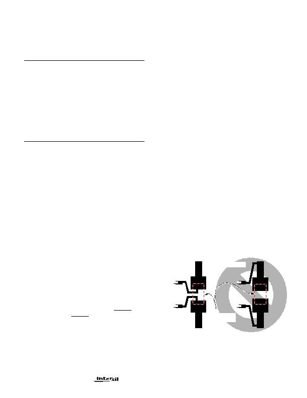
FIGURE 1. SENSE RESISTOR PCB LAYOUT
R
ISET
ISL6161
相关PDF资料 |
PDF描述 |
|---|---|
| NCV8535MN300R2G | IC REG LDO 3V .7A 10-DFN |
| VE-JTH-CY-B1 | CONVERTER MOD DC/DC 52V 50W |
| VI-BWX-CV-S | CONVERTER MOD DC/DC 5.2V 150W |
| T86D476M016EAAS | CAP TANT 47UF 16V 20% 2917 |
| TLCL226M006XTA | CAP TANT 22UF 6.3V 20% 0603 |
相关代理商/技术参数 |
参数描述 |
|---|---|
| ISL6161IBZA | 功能描述:IC CTRLR PWR DISTRIB DUAL 14SOIC RoHS:是 类别:集成电路 (IC) >> PMIC - 热交换 系列:- 产品培训模块:Obsolescence Mitigation Program 标准包装:100 系列:- 类型:热插拔开关 应用:通用 内部开关:是 电流限制:可调 电源电压:9 V ~ 13.2 V 工作温度:-40°C ~ 150°C 安装类型:表面贴装 封装/外壳:10-WFDFN 裸露焊盘 供应商设备封装:10-TDFN-EP(3x3) 包装:管件 |
| ISL6161IBZA-T | 功能描述:IC CTRLR PWR DISTRIB DUAL 14SOIC RoHS:是 类别:集成电路 (IC) >> PMIC - 热交换 系列:- 产品培训模块:Obsolescence Mitigation Program 标准包装:100 系列:- 类型:热插拔开关 应用:通用 内部开关:是 电流限制:可调 电源电压:9 V ~ 13.2 V 工作温度:-40°C ~ 150°C 安装类型:表面贴装 封装/外壳:10-WFDFN 裸露焊盘 供应商设备封装:10-TDFN-EP(3x3) 包装:管件 |
| ISL6172DRZA | 功能描述:热插拔功率分布 W/ANNEAL DL LV HOT SWAP CNTRLR 0-85 TMP RoHS:否 制造商:Texas Instruments 产品:Controllers & Switches 电流限制: 电源电压-最大:7 V 电源电压-最小:- 0.3 V 工作温度范围: 功率耗散: 安装风格:SMD/SMT 封装 / 箱体:MSOP-8 封装:Tube |
| ISL6172DRZA-T | 功能描述:热插拔功率分布 W/ANNEAL DL LV HOT SWAP CNTRLR 0-85 TMP RoHS:否 制造商:Texas Instruments 产品:Controllers & Switches 电流限制: 电源电压-最大:7 V 电源电压-最小:- 0.3 V 工作温度范围: 功率耗散: 安装风格:SMD/SMT 封装 / 箱体:MSOP-8 封装:Tube |
| ISL6173 | 制造商:INTERSIL 制造商全称:Intersil Corporation 功能描述:Dual Low Voltage Hot Swap Controller |
发布紧急采购,3分钟左右您将得到回复。