- 您现在的位置:买卖IC网 > PDF目录383141 > ISL6161CBZA (INTERSIL CORP) Octal D-Type Transparent Latches With 3-State Outputs 20-TSSOP -40 to 85 PDF资料下载
参数资料
| 型号: | ISL6161CBZA |
| 厂商: | INTERSIL CORP |
| 元件分类: | 电源管理 |
| 英文描述: | Octal D-Type Transparent Latches With 3-State Outputs 20-TSSOP -40 to 85 |
| 中文描述: | 2-CHANNEL POWER SUPPLY SUPPORT CKT, PDSO14 |
| 封装: | LEAD FREE, PLASTIC, MS-012AB, SOIC-14 |
| 文件页数: | 6/10页 |
| 文件大小: | 224K |
| 代理商: | ISL6161CBZA |
6
The ISL6161 responds to a load short (defined as a current
level 3X the OC set point with a fast transition) by
immediately driving the relevant N-Channel MOSFET gate to
0V in ~3
μ
s. The gate voltage is then slowly ramped up soft
starting the N-Channel MOSFET to the programmed current
regulation limit level, this is the start of the time out period if
the abnormal load condition still exists. The programmed
current regulation level is held until either the OC event
passes or the time out period expires. If the former is the
case then the N-Channel MOSFET is fully enhanced and the
C
TIM
charging current is diverted away from the capacitor. If
the time out period expires prior to OC resolution then both
gates are quickly pulled to 0V turning off both N-Channel
MOSFETs simultaneously.
Upon any UV condition the PGOOD signal will pull low when
tied high through a resistor to the logic supply. This pin is a
fault indicator but not the OC latch off indicator. For an OC
latch off indication, monitor CTIM, pin 10. This pin will rise
rapidly to 12V once the time out period expires. See block
diagram for OC latch off circuit suggestion.
The ISL6161 is reset by a rising edge on the ENABLE pin
and is turned on by the ENABLE pin being driven low.
ISL6161 Application Considerations
In a non PCI-Express, motor drive application
Current loop
stabilization
is facilitated through a small value resistor in
series with the gate timing capacitor. As the ISL6161 drives
a highly inductive current load, instability characterized by
the gate voltage repeatedly ramping up and down may
appear. A simple method to enhance stability is provided by
the substitution of a larger value gate resistor. Typically this
situation can be avoided by eliminating long point to point
wiring to the load.
With the ENABLE internal pull-up the ISL6161 is well suited
for implementation on either side of the connector where a
motherboard prebiased condition or a load board staggered
connection is present. In either case the ISL6161 turns on in
a soft start mode protecting the supply rail from sudden
current loading.
During the
Time Out delay period
with the ISL6161 in
current limit mode, the V
GS
of the external N-Channel
MOSFETs is reduced driving the N-Channel MOSFET
switch into a high r
DS(ON)
state. Thus avoid extended time
out periods as the external N-Channel MOSFETs may be
damaged or destroyed due to excessive internal power
dissipation. Refer to the MOSFET manufacturers data sheet
for SOA information.
With the high levels of inrush current e.g., highly capacitive
loads and motor start up currents,
choosing the current
regulation (CR) level
is crucial to provide both protection
and still allow for this inrush current without latching off.
Consider this in addition to the time out delay when choosing
MOSFETs for your design.
Physical layout of Rsense resistors
is critical to avoid
inadvertently lowering the CR and trip levels. Ideally trace
routing between the Rsense resistors and the ISL6161 is
direct and as short as possible with zero current in the sense
lines.
Open load detection
can be accomplished by monitoring
the ISEN pins. Although gated off the external FET I
DSS
will
cause the ISEN pin to float above ground to some voltage
when there is no attached load. If this is not desired 5K
resistors from the xISEN pins to ground will prevent the
outputs from floating when the external switch FETs are
disabled and the outputs are open.
For
PCI-Express applications
the ISL6161 and the
ISL6118 provide the fundamental hotswap function for the
+12V & +3.3V main rails and the +3.3V aux respectively as
shown in Figure 13.
X4/X8
10
30, 3.3
40, 2.5
100
4.99
15, 3.5
20, 2.6
53
X16
10
30, 3.3
16, 6.3
100
4.99
15, 3.5
8, 6.6
53
NOTE: Nominal CR Vth = Rilim x 10
μ
A.
TABLE 2.
C
TIM
CAPACITOR
NOMINAL TIME OUT PERIOD
0.022
μ
F
4.4ms
0.047
μ
F
9.4ms
0.1
μ
F
20ms
NOTE: Nominal time-out period in seconds = C
TIM
x 200k
.
TABLE 1. (Continued)
PCI-EXPRESS
ADD-IN CARD
CONNECTOR
R
ILIM
(k
)
3.3V R
SENSE
(m
),
NOMINAL
CR (A)
12V R
SENSE
(m
),
NOMINAL
CR (A)
NOMINAL
CRVth
(mV)
CORRECT
TO ISEN AND
CURRENT
SENSE RESISTOR
INCORRECT
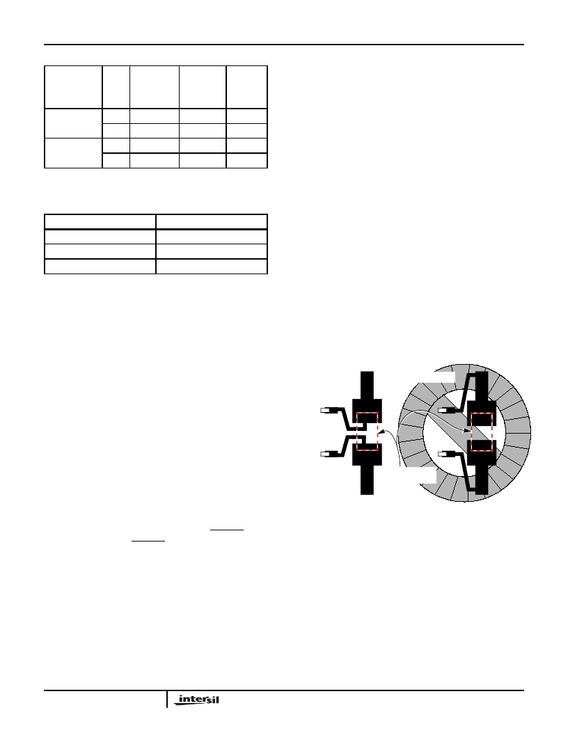
FIGURE 1. SENSE RESISTOR PCB LAYOUT
R
ISET
ISL6161
相关PDF资料 |
PDF描述 |
|---|---|
| ISL6161CBZA-T | Octal D-Type Transparent Latches With 3-State Outputs 20-TSSOP -40 to 85 |
| ISL6173DRZA | Dual Low Voltage Hot Swap Controller |
| ISL6173 | Dual Low Voltage Hot Swap Controller |
| ISL6173EVAL3 | Dual Low Voltage Hot Swap Controller |
| ISL6173DRZA-T | Dual Low Voltage Hot Swap Controller |
相关代理商/技术参数 |
参数描述 |
|---|---|
| ISL6161CBZA-T | 功能描述:IC CTLR PWR DISTRIB DUAL 14SOIC RoHS:是 类别:集成电路 (IC) >> PMIC - 热交换 系列:- 产品培训模块:Lead (SnPb) Finish for COTS Obsolescence Mitigation Program 标准包装:119 系列:- 类型:热交换控制器 应用:通用型,PCI Express? 内部开关:无 电流限制:- 电源电压:3.3V,12V 工作温度:-40°C ~ 85°C 安装类型:表面贴装 封装/外壳:80-TQFP 供应商设备封装:80-TQFP(12x12) 包装:托盘 产品目录页面:1423 (CN2011-ZH PDF) |
| ISL6161IBZA | 功能描述:IC CTRLR PWR DISTRIB DUAL 14SOIC RoHS:是 类别:集成电路 (IC) >> PMIC - 热交换 系列:- 产品培训模块:Obsolescence Mitigation Program 标准包装:100 系列:- 类型:热插拔开关 应用:通用 内部开关:是 电流限制:可调 电源电压:9 V ~ 13.2 V 工作温度:-40°C ~ 150°C 安装类型:表面贴装 封装/外壳:10-WFDFN 裸露焊盘 供应商设备封装:10-TDFN-EP(3x3) 包装:管件 |
| ISL6161IBZA-T | 功能描述:IC CTRLR PWR DISTRIB DUAL 14SOIC RoHS:是 类别:集成电路 (IC) >> PMIC - 热交换 系列:- 产品培训模块:Obsolescence Mitigation Program 标准包装:100 系列:- 类型:热插拔开关 应用:通用 内部开关:是 电流限制:可调 电源电压:9 V ~ 13.2 V 工作温度:-40°C ~ 150°C 安装类型:表面贴装 封装/外壳:10-WFDFN 裸露焊盘 供应商设备封装:10-TDFN-EP(3x3) 包装:管件 |
| ISL6172DRZA | 功能描述:热插拔功率分布 W/ANNEAL DL LV HOT SWAP CNTRLR 0-85 TMP RoHS:否 制造商:Texas Instruments 产品:Controllers & Switches 电流限制: 电源电压-最大:7 V 电源电压-最小:- 0.3 V 工作温度范围: 功率耗散: 安装风格:SMD/SMT 封装 / 箱体:MSOP-8 封装:Tube |
| ISL6172DRZA-T | 功能描述:热插拔功率分布 W/ANNEAL DL LV HOT SWAP CNTRLR 0-85 TMP RoHS:否 制造商:Texas Instruments 产品:Controllers & Switches 电流限制: 电源电压-最大:7 V 电源电压-最小:- 0.3 V 工作温度范围: 功率耗散: 安装风格:SMD/SMT 封装 / 箱体:MSOP-8 封装:Tube |
发布紧急采购,3分钟左右您将得到回复。