- 您现在的位置:买卖IC网 > PDF目录22093 > ISL61863AIRZ-T (Intersil)IC USB PWR CTRLR 1.5A 10DFN PDF资料下载
参数资料
| 型号: | ISL61863AIRZ-T |
| 厂商: | Intersil |
| 文件页数: | 13/18页 |
| 文件大小: | 717K |
| 描述: | IC USB PWR CTRLR 1.5A 10DFN |
| 标准包装: | 6,000 |
| 类型: | 热交换开关 |
| 应用: | USB 过电流保护控制器 |
| 内部开关: | 是 |
| 电流限制: | 1.5A |
| 电源电压: | 2.5 V ~ 5.5 V |
| 工作温度: | -40°C ~ 85°C |
| 安装类型: | 表面贴装 |
| 封装/外壳: | 10-VFDFN 裸露焊盘 |
| 供应商设备封装: | 10-DFN(3x3) |
| 包装: | 带卷 (TR) |
ISL6186
13
FN7698.2
November 3, 2011
Application Information
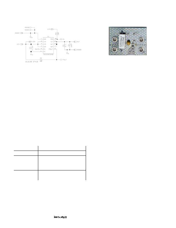
Using the ISL6186XEVAL1Z Platform
General and Biasing Information
There are three evaluation platforms for the ISL6186 family.
There is one for each package style, each with a different
continuous output current level and representing a mix of enable
polarity and output retry or latch options. The standard available
evaluation board options are listed at the end of the Ordering
Information table, which starts on page3. Figure 28A illustrates
the schematic for the 10 Ld DFN ISL61863EVAL1Z. Other than
the unique PGOOD output on the ISL61863 types, all the
schematics and functions are the same across all three package
types. Consult the individual package pinouts on page2 for those
differences.
The evaluation platform is biased and monitored through a few
labeled test points. See Table 1 for test point assignments and
descriptions.
Upon proper bias of the evaluation platform and correct enabling
of the IC, the ISL6186 will have a nominal V
IN
/5.1?/SPAN> load current
that is below the continuous current rating passing through each
enabled switch. See Figures 14 to 16 for typical ISL6186 turn-on
and turn-off waveforms.
External current loading in excess of the trip current level for the
particular part being evaluated will result in the ISL6186 entering
current limiting mode. Figure 11 illustrates current limiting mode
for the ISL6186 product variants with 1.5A of continuous load
current rating. The scope shot shows current limiting for ~12ms
before it is turned off and the fault signal is asserted.
Application Considerations
See Table 2 for a listing of the ISL6186XEVAL1Z board
components.
Decoupling V
IN
Application considerations for the ISL6186 family are widely
accepted best industry practices. Good decoupling practices on
the V
IN
pin must be followed by placement close to the IC, with at
least 2.2礔 being recommended. For the 3.0 and 3.6A versions,
at least 33礔 is recommended to prevent spiking and glitching
on V
IN
during an OC event. Use good PCB layout practices to
reduce input and output inductance to the ISL6186.
Loading V
OUT
When designing with the 3A and 3.6A versions in an
implementation in which the output may be unloaded (open)
while the ISL6186 is turned on, a minimum of 4.7礔 of
capacitive loading is recommended to prevent high dv/dt from
unnecessarily activating the surge/ESD circuitry.
Continuous Current Ratings
The ISL6186 provides several continuous current rated devices
specified at V
IN
= 5V: these are the 1.5A, 3A and 3.6A options,
which are capable over the entire temperature extreme. At
V
IN
=3.3V, current capability is degraded, and the ISL6186 is
specified at 1.5A and 3A. At V
IN
= 2.5V, there are no
specifications, but a typical value is provided in the specification
table as guidance for +25癈 operation. This degraded capability
is due to the higher r
DS(ON)
of the FET switch at the lower bias
voltage.
Enhanced thermal characteristics and an increased number of
bond wires allows the 10 Ld DFN to have a higher current
capability than either the 8 Ld SOIC or 8 Ld DFN.
ISL61863EVAL1Z Schematic and Photo
FIGURE 28A. ISL61863EVAL1Z SCHEMATIC
FIGURE 28B. ISL61863EVAL1Z BOARD PHOTO
FIGURE 28. ISL61863EVAL1Z SCHEMATIC and ISL61863EVAL1Z PHOTOGRAPH
*
NOTE: *PGD Output only available on ISL61863 types
GND
VIN
GND
OUT
FLT
EN
PG
TABLE 1. ISL61863EVAL1Z TEST POINT ASSIGNMENTS
TP NAME
DESCRIPTION
GND
Eval Board and IC Gnd
VIN
Eval Board, IC Bias and Power Input
EN
Enable Switch
OUT
Switch Power Output
PG
Power-Good Output
FLT
Fault Output
相关PDF资料 |
PDF描述 |
|---|---|
| MIC5201-5.0BM | IC REG LDO 5V .2A 8SOIC |
| GMM06DSEH-S13 | CONN EDGECARD 12POS .156 EXTEND |
| HHR-900DA01L2X4 | BATTERY PACK 9.6V 8250MAH NIMH |
| ISL61863ICRZ-T | IC USB PWR CTRLR 3.6A 10DFN |
| HSC43DREN | CONN EDGECARD 86POS .100 EYELET |
相关代理商/技术参数 |
参数描述 |
|---|---|
| ISL61863BCRZ | 功能描述:热插拔功率分布 SINGLE USB HOTSWAP 5A/RETRY 3X3 10LD RoHS:否 制造商:Texas Instruments 产品:Controllers & Switches 电流限制: 电源电压-最大:7 V 电源电压-最小:- 0.3 V 工作温度范围: 功率耗散: 安装风格:SMD/SMT 封装 / 箱体:MSOP-8 封装:Tube |
| ISL61863BCRZ-T | 功能描述:热插拔功率分布 SINGLE USB HOTSWAP 5A/RETRY 3X3 10LD RoHS:否 制造商:Texas Instruments 产品:Controllers & Switches 电流限制: 电源电压-最大:7 V 电源电压-最小:- 0.3 V 工作温度范围: 功率耗散: 安装风格:SMD/SMT 封装 / 箱体:MSOP-8 封装:Tube |
| ISL61863BIRZ | 功能描述:热插拔功率分布 SINGLE USB HOTSWAP 5A/RETRY 3X3 10LD RoHS:否 制造商:Texas Instruments 产品:Controllers & Switches 电流限制: 电源电压-最大:7 V 电源电压-最小:- 0.3 V 工作温度范围: 功率耗散: 安装风格:SMD/SMT 封装 / 箱体:MSOP-8 封装:Tube |
| ISL61863BIRZ-T | 功能描述:热插拔功率分布 SINGLE USB HOTSWAP 5A/RETRY 3X3 10LD RoHS:否 制造商:Texas Instruments 产品:Controllers & Switches 电流限制: 电源电压-最大:7 V 电源电压-最小:- 0.3 V 工作温度范围: 功率耗散: 安装风格:SMD/SMT 封装 / 箱体:MSOP-8 封装:Tube |
| ISL61863CCRZ | 功能描述:热插拔功率分布 SINGLE USB HOTSWAP /I3A/LATCH 3X3 10LD RoHS:否 制造商:Texas Instruments 产品:Controllers & Switches 电流限制: 电源电压-最大:7 V 电源电压-最小:- 0.3 V 工作温度范围: 功率耗散: 安装风格:SMD/SMT 封装 / 箱体:MSOP-8 封装:Tube |
发布紧急采购,3分钟左右您将得到回复。