- 您现在的位置:买卖IC网 > PDF目录20665 > ISL6263CEVAL1 (Intersil)EVAL BOARD 1 FOR ISL6263C PDF资料下载
参数资料
| 型号: | ISL6263CEVAL1 |
| 厂商: | Intersil |
| 文件页数: | 16/18页 |
| 文件大小: | 0K |
| 描述: | EVAL BOARD 1 FOR ISL6263C |
| 标准包装: | 1 |
| 系列: | * |
�� �
�
�ISL6263C�
�Dynamic� Mode� of� Operation� -� Compensation�
�Parameters�
�Intersil� provides� a� spreadsheet� to� calculate� the� compensator�
�parameters.� Caution� needs� to� be� used� in� choosing� the� input�
�resistor� to� the� FB� pin.� Excessively� high� resistance� will� cause�
�an� error� to� the� output� voltage� regulation� due� to� the� bias�
�current� flowing� through� the� FB� pin.� It� is� recommended� to�
�keep� this� resistor� below� 3k� ?� .�
�Layout� Considerations�
�As� a� general� rule,� power� should� be� on� the� bottom� layer� of�
�the� PCB� and� weak� analog� or� logic� signals� are� on� the� top�
�layer� of� the� PCB.� The� ground-plane� layer� should� be� adjacent�
�to� the� top� layer� to� provide� shielding.�
�Inductor� Current� Sense� and� the� NTC� Placement�
�It� is� crucial� that� the� inductor� current� be� sensed� directly� at� the�
�PCB� pads� of� the� sense� element,� be� it� DCR� sensed� or� discrete�
�resistor� sensed.� The� effect� of� the� NTC� on� the� inductor� DCR�
�thermal� drift� is� directly� proportional� to� its� thermal� coupling� with�
�the� inductor� and� thus,� the� physical� proximity� to� it.�
�Signal� Ground� and� Power� Ground�
�The� ground� plane� layer� should� have� a� single� point� connection�
�to� the� analog� ground� at� the� VSS� pin.� The� VSS� island� should�
�be� located� under� the� IC� package� along� with� the� weak� analog�
�traces� and� components.� The� paddle� on� the� bottom� of� the�
�ISL6263C� QFN� package� is� not� electrically� connected� to� the�
�IC,� however,� it� is� recommended� to� make� a� good� thermal�
�connection� to� the� VSS� island� using� several� vias.� Connect� the�
�input� capacitors,� the� output� capacitors,� and� the� source� of� the�
�lower� MOSFETs� to� the� power� ground� plane.�
�LGATE,� PVCC,� and� PGND�
�PGND� is� the� return� path� for� the� pull-down� of� the� LGATE�
�low-side� MOSFET� gate� driver.� Ideally,� PGND� should� be�
�connected� to� the� source� of� the� low-side� MOSFET� with� a�
�low-resistance,� low-inductance� path.� The� LGATE� trace� should�
�be� routed� in� parallel� with� the� trace� from� the� PGND� pin.� These�
�two� traces� should� be� short,� wide,� and� away� from� other� traces�
�because� of� the� high� peak� current� and� extremely� fast� dv/dt.�
�PVCC� should� be� decoupled� to� PGND� with� a� ceramic� capacitor�
�physically� located� as� close� as� practical� to� the� IC� pins.�
�UGATE,� BOOT,� and� PHASE�
�PHASE� is� the� return� path� for� the� entire� UGATE� high-side�
�MOSFET� gate� driver.� The� layout� for� these� signals� require�
�similar� treatment,� but� to� a� greater� extent,� than� those� for�
�LGATE,� PVCC,� and� PGND.� These� signals� swing� from�
�approximately� VIN� to� VSS� and� are� more� likely� to� couple� into�
�other� signals.�
�VSEN� and� RTN�
�These� traces� should� be� laid� out� as� noise� sensitive.� For�
�optimum� load� line� regulation� performance,� the� traces�
�connecting� these� two� pins� to� the� Kelvin� sense� leads� of� the�
�processor� should� be� laid� out� away� from� rapidly� rising� voltage�
�nodes,� (switching� nodes)� and� other� noisy� traces.� The� filter�
�capacitors� C� FILTER1� ,� C� FILTER2� ,� and� C� FILTER3� used� in�
�conjunction� with� filter� resistors� R� FILTER1� and� R� FILTER2� form�
�common� mode� and� differential� mode� filters,� as� shown� in�
�Figure� 8.� The� noise� environment� of� the� application� and�
�actual� board� layout� conditions� will� drive� the� extent� of� filter�
�complexity.� The� maximum� recommended� resistance� for�
�R� FILTER1� and� R� FILTER2� is� approximately� 10� ?� to� avoid�
�interaction� with� the� 50k� ?� input� resistance� of� the� remote�
�sense� differential� amplifier.� The� physical� location� of� these�
�resistors� is� not� as� critical� as� the� filter� capacitors.� Typical�
�capacitance� values� for� C� FILTER1� ,� C� FILTER2� ,� and� C� FILTER3�
�range� between� 330pF� to� 1000pF� and� should� be� placed� near�
�the� IC.�
�RBIAS�
�The� resistor� R� RBIAS� should� be� placed� in� close� proximity� to�
�the� ISL6263C� using� a� noise-free� current� return� path� to� the�
�VSS� pin.�
�IMON,� SOFT,� OCSET,� V� W,� COMP,� FB,� VDIFF,�
�ICOMP,� ISP,� ISN� and� VO�
�The� traces� and� components� associated� with� these� pins�
�require� close� proximity� to� the� IC� as� well� as� close� proximity� to�
�each� other.� This� section� of� the� converter� circuit� needs� to� be�
�located� above� the� island� of� analog� ground� with� the�
�single-point� connection� to� the� VSS� pin.�
�Resistor� R� S�
�Resistor� R� S� is� preferably� located� near� the� boundary�
�between� the� power� ground� and� the� island� of� analog� ground�
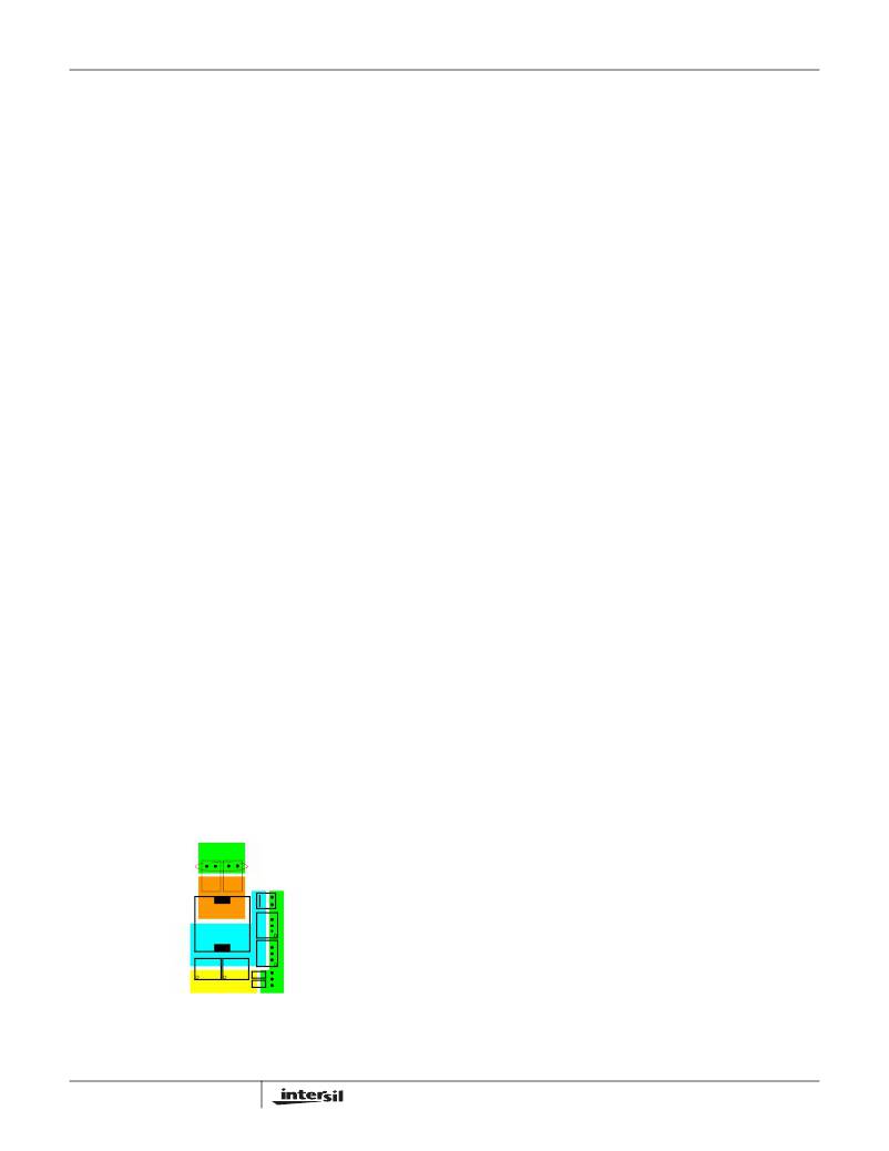
�VIAS� TO�
�GROUND�
�PLANE�
�GND�
�OUTPUT�
�CAPACITORS�
�SCHOTTKY�
�connected� to� the� VSS� pin.�
�VID<0:4>,� AF_EN,� PGOOD,� and� VR_ON�
�These� are� logic� signals� that� do� not� require� special� attention.�
�INDUCTOR�
�HIGH-SIDE�
�MOSFETS�
�VOUT�
�PHASE�
�NODE�
�VIN�
�DIODE�
�LOW-SIDE�
�MOSFETS�
�INPUT�
�CAPACITORS�
�FDE�
�This� logic� signal� should� be� treated� as� noise� sensitive� and�
�should� be� routed� away� from� rapidly� rising� voltage� nodes,�
�(switching� nodes)� and� other� noisy� traces.�
�FIGURE� 10.� TYPICAL� POWER� COMPONENT� PLACEMENT�
�16�
�VIN�
�The� VIN� signal� should� be� connected� near� the� drain� of� the�
�high-side� MOSFET.�
�FN6745.1�
�July� 8,� 2010�
�相关PDF资料 |
PDF描述 |
|---|---|
| AISC-1008F-6R8G-T | INDUCTOR 6800NH 360MA 2% SMD |
| MAX4211AEUE+T | IC CURRENT MONITOR 1.5% 16TSSOP |
| TC1303A-ZS0EUNTR | IC REG DL BCK/LINEAR SYNC 10MSOP |
| VI-J6N-EW-B1 | CONVERTER MOD DC/DC 18.5V 100W |
| ISL6620CRZ-T | IC MOSFET DVR SYNC BUCK 10-DFN |
相关代理商/技术参数 |
参数描述 |
|---|---|
| ISL6263CHRZ | 功能描述:直流/直流开关调节器 1-PHS INT DC/DC BUCK CNTRLR IMVP-6 W/IMON RoHS:否 制造商:International Rectifier 最大输入电压:21 V 开关频率:1.5 MHz 输出电压:0.5 V to 0.86 V 输出电流:4 A 输出端数量: 最大工作温度: 安装风格:SMD/SMT 封装 / 箱体:PQFN 4 x 5 |
| ISL6263CHRZ-T | 功能描述:直流/直流开关调节器 1-PHS INT DC/DC BUCK CNTRLR IMVP-6 W/IMON RoHS:否 制造商:International Rectifier 最大输入电压:21 V 开关频率:1.5 MHz 输出电压:0.5 V to 0.86 V 输出电流:4 A 输出端数量: 最大工作温度: 安装风格:SMD/SMT 封装 / 箱体:PQFN 4 x 5 |
| ISL6263CRZ | 功能描述:直流/直流开关调节器 1 PHS INT DC/DC BUCK CNTRLR FOR INTEL RoHS:否 制造商:International Rectifier 最大输入电压:21 V 开关频率:1.5 MHz 输出电压:0.5 V to 0.86 V 输出电流:4 A 输出端数量: 最大工作温度: 安装风格:SMD/SMT 封装 / 箱体:PQFN 4 x 5 |
| ISL6263CRZ-T | 功能描述:直流/直流开关调节器 1 PHS INT DC/DC BUCK CNTRLR FOR INTEL RoHS:否 制造商:International Rectifier 最大输入电压:21 V 开关频率:1.5 MHz 输出电压:0.5 V to 0.86 V 输出电流:4 A 输出端数量: 最大工作温度: 安装风格:SMD/SMT 封装 / 箱体:PQFN 4 x 5 |
| ISL6263DEVAL1Z | 功能描述:EVAL BAORD 1 FOR ISL6263D RoHS:是 类别:编程器,开发系统 >> 评估板 - DC/DC 与 AC/DC(离线)SMPS 系列:* 产品培训模块:Obsolescence Mitigation Program 标准包装:1 系列:True Shutdown™ 主要目的:DC/DC,步升 输出及类型:1,非隔离 功率 - 输出:- 输出电压:- 电流 - 输出:1A 输入电压:2.5 V ~ 5.5 V 稳压器拓扑结构:升压 频率 - 开关:3MHz 板类型:完全填充 已供物品:板 已用 IC / 零件:MAX8969 |
发布紧急采购,3分钟左右您将得到回复。