参数资料
| 型号: | ISL62881BHRTZ-T |
| 厂商: | Intersil |
| 文件页数: | 18/35页 |
| 文件大小: | 0K |
| 描述: | IC REG PWM SGL PHASE 32TQFN |
| 标准包装: | 6,000 |
| 应用: | 控制器,Intel IMVP-6.5? |
| 输入电压: | 5 V ~ 25 V |
| 输出数: | 1 |
| 输出电压: | 0.013 V ~ 1.5 V |
| 工作温度: | -10°C ~ 100°C |
| 安装类型: | 表面贴装 |
| 封装/外壳: | 32-WFQFN 裸露焊盘 |
| 供应商设备封装: | 32-TQFN-EP(5x5) |
| 包装: | 带卷 (TR) |
第1页第2页第3页第4页第5页第6页第7页第8页第9页第10页第11页第12页第13页第14页第15页第16页第17页当前第18页第19页第20页第21页第22页第23页第24页第25页第26页第27页第28页第29页第30页第31页第32页第33页第34页第35页
�� �
�
�ISL62881,� ISL62881B�
�Overshoot� Reduction� Function�
�The� ISL62881� has� an� optional� overshoot� reduction� function,�
�enabled� or� disabled� by� the� resistor� from� the� COMP� pin� to� GND,� as�
�shown� in� Table� 3.�
�Inductor� DCR� Current-Sensing� Network�
�PHASE�
�When� a� load� release� occurs,� the� energy� stored� in� the� inductors�
�will� dump� to� the� output� capacitor,� causing� output� voltage�
�overshoot.� The� inductor� current� freewheels� through� the� low-side�
�RSUM�
�ISUM+�
�MOSFET� during� this� period� of� time.� The� overshoot� reduction�
�function� turns� off� the� low-side� MOSFET� during� the� output� voltage�
�L�
�RNTCS�
�+�
�overshoot,� forcing� the� inductor� current� to� freewheel� through� the�
�low-side� MOSFET� body� diode.� Since� the� body� diode� voltage� drop�
�is� much� higher� than� MOSFET� R� DS(ON)� voltage� drop,� more� energy�
�is� dissipated� on� the� low-side� MOSFET� therefore� the� output�
�voltage� overshoot� is� lower.�
�DCR�
�RNTC�
�RP�
�CN� VCN�
�-�
�RI�
�ISUM-�
�If� the� overshoot� reduction� function� is� enabled,� the� ISL62881�
�monitors� the� COMP� pin� voltage� to� determine� the� output� voltage�
�overshoot� condition.� The� COMP� voltage� will� fall� and� hit� the� clamp�
�voltage� when� the� output� voltage� overshoots.� The� ISL62881� will�
�turn� off� LGATE� when� COMP� is� being� clamped.� The� low-side�
�MOSFET� in� the� power� stage� will� be� turned� off.� When� the� output�
�voltage� has� reached� its� peak� and� starts� to� come� down,� the� COMP�
�voltage� starts� to� rise� and� is� no� longer� clamped.� The� ISL62881� will�
�resume� normal� PWM� operation.�
�While� the� overshoot� reduction� function� reduces� the� output�
�voltage� overshoot,� energy� is� dissipated� on� the� low-side� MOSFET,�
�causing� additional� power� loss.� The� more� frequent� the� transient�
�event,� the� more� power� loss� is� dissipated� on� the� low-side� MOSFET.�
�The� MOSFET� may� face� severe� thermal� stress� when� transient�
�events� happen� at� a� high� repetitive� rate.� User� discretion� is� advised�
�when� this� function� is� enabled.�
�IO�
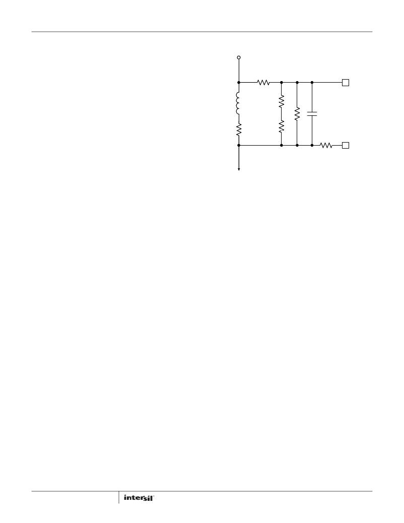
�FIGURE� 13.� DCR� CURRENT-SENSING� NETWORK�
�Figure� 13� shows� the� inductor� DCR� current-sensing� network� for� a�
�2-phase� solution.� An� inductor� current� flows� through� the� DCR� and�
�creates� a� voltage� drop.� The� inductor� has� a� resistors� in� R� sum�
�connected� to� the� phase-node-side� pad� and� a� PCB� trace�
�connected� to� the� output-side� pad� to� accurately� sense� the�
�inductor� current� by� sensing� the� DCR� voltage� drop.� The� sensed�
�current� information� is� fed� to� the� NTC� network� (consisting� of�
�R� ntcs� ,� R� ntc� and� R� p� )� and� capacitor� C� n� .� R� ntc� is� a� negative�
�temperature� coefficient� (NTC)� thermistor,� used� to�
�temperature-compensate� the� inductor� DCR� change.� The� inductor�
�current� information� is� presented� to� the� capacitor� C� n� .� Equations� 7�
�through� 11� describe� the� frequency-domain� relationship� between�
�V� Cn� (� s� )� =� ?� -----------------------------------------� � DCR� ?� � I� o� (� s� )� � A� cs� (� s� )�
�R� ntcnet� =� ---------------------------------------------------�
�1� +� ------�
�ω� L�
�ω� sns�
�ω� L� =� ------------�
�Key� Component� Selection�
�R� BIAS�
�The� ISL62881� uses� a� resistor� (1%� or� better� tolerance� is�
�recommended)� from� the� RBIAS� pin� to� GND� to� establish� highly�
�accurate� reference� current� sources� inside� the� IC.� Using�
�R� BIAS� =� 147k� Ω� sets� the� controller� for� CPU� core� application� and�
�using� R� BIAS� =� 47k� Ω� sets� the� controller� for� GPU� core� application.�
�Do� not� connect� any� other� components� to� this� pin.� Do� not� connect�
�any� capacitor� to� the� RBIAS� pin� as� it� will� create� instability.�
�Care� should� be� taken� in� layout� that� the� resistor� is� placed� very�
�close� to� the� RBIAS� pin� and� that� a� good� quality� signal� ground� is�
�connected� to� the� opposite� side� of� the� R� BIAS� resistor.�
�R� is� and� C� is�
�inductor� total� current� I� o� (s)� and� C� n� voltage� V� Cn� (s):�
�?� R� ntcnet� ?�
�?� R� ntcnet� +� R� sum� ?�
�(� R� ntcs� +� R� ntc� )� � R� p�
�R� ntcs� +� R� ntc� +� R� p�
�s�
�s�
�A� cs� (� s� )� =� ----------------------�
�1� +� ------------�
�DCR�
�L�
�(EQ.� 7)�
�(EQ.� 8)�
�(EQ.� 9)�
�(EQ.� 10)�
�ω� sns� =� ------------------------------------------------------�
�-----------------------------------------� � C� n�
�As� Figures� 1� and� 2� show,� the� ISL62881� needs� the�
�R� is� -� C� is� network� across� the� ISUM+� and� the� ISUM-� pins� to� stabilize�
�the� droop� amplifier.� The� preferred� values� are� R� is� =� 82.5� Ω� and�
�C� is� =� 0.01μF.� Slight� deviations� from� the� recommended� values� are�
�acceptable.� Large� deviations� may� result� in� instability.�
�18�
�1� (EQ.� 11)�
�R� ntcnet� � R� sum�
�R� ntcnet� +� R� sum�
�Transfer� function� A� cs� (s)� always� has� unity� gain� at� DC.� The� inductor�
�DCR� value� increases� as� the� winding� temperature� increases,�
�giving� higher� reading� of� the� inductor� DC� current.� The� NTC� R� ntc�
�values� decreases� as� its� temperature� decreases.� Proper�
�selections� of� R� sum� ,� R� ntcs� ,� R� p� and� R� ntc� parameters� ensure� that�
�V� Cn� represents� the� inductor� total� DC� current� over� the�
�temperature� range� of� interest.�
�FN6924.3�
�June� 16,� 2011�
�相关PDF资料 |
PDF描述 |
|---|---|
| UWP1A470MCL1GB | CAP ALUM 47UF 10V 20% SMD |
| GMM15DRTS | CONN EDGECARD 30POS DIP .156 SLD |
| RBC50DRYH-S734 | CONN EDGECARD 100PS DIP .100 SLD |
| ACM15DRSI | CONN EDGECARD 30POS DIP .156 SLD |
| RBB34DHBN | CONN EDGECARD 68POS R/A .050 DIP |
相关代理商/技术参数 |
参数描述 |
|---|---|
| ISL62881C | 制造商:INTERSIL 制造商全称:Intersil Corporation 功能描述:Single-Phase PWM Regulator for IMVP-6.5a?¢ Mobile CPUs and GPUs |
| ISL62881CCPUEVAL2Z | 功能描述:EVAL BOARD ISL62881CCPU 28QFN RoHS:是 类别:编程器,开发系统 >> 评估板 - DC/DC 与 AC/DC(离线)SMPS 系列:- 产品培训模块:Obsolescence Mitigation Program 标准包装:1 系列:True Shutdown™ 主要目的:DC/DC,步升 输出及类型:1,非隔离 功率 - 输出:- 输出电压:- 电流 - 输出:1A 输入电压:2.5 V ~ 5.5 V 稳压器拓扑结构:升压 频率 - 开关:3MHz 板类型:完全填充 已供物品:板 已用 IC / 零件:MAX8969 |
| ISL62881CGPUEVAL2Z | 功能描述:EVAL BOARD FOR ISL62881C RoHS:是 类别:编程器,开发系统 >> 评估板 - DC/DC 与 AC/DC(离线)SMPS 系列:- 产品培训模块:Obsolescence Mitigation Program 标准包装:1 系列:True Shutdown™ 主要目的:DC/DC,步升 输出及类型:1,非隔离 功率 - 输出:- 输出电压:- 电流 - 输出:1A 输入电压:2.5 V ~ 5.5 V 稳压器拓扑结构:升压 频率 - 开关:3MHz 板类型:完全填充 已供物品:板 已用 IC / 零件:MAX8969 |
| ISL62881CHRTZ | 功能描述:直流/直流开关调节器 1-PHS PWM BUCKG FOR MICROPROC PWR SUPPLY RoHS:否 制造商:International Rectifier 最大输入电压:21 V 开关频率:1.5 MHz 输出电压:0.5 V to 0.86 V 输出电流:4 A 输出端数量: 最大工作温度: 安装风格:SMD/SMT 封装 / 箱体:PQFN 4 x 5 |
| ISL62881CHRTZ-T | 功能描述:直流/直流开关调节器 1-PHS PWM BUCKG FOR MICROPROC PWR SUPPLY RoHS:否 制造商:International Rectifier 最大输入电压:21 V 开关频率:1.5 MHz 输出电压:0.5 V to 0.86 V 输出电流:4 A 输出端数量: 最大工作温度: 安装风格:SMD/SMT 封装 / 箱体:PQFN 4 x 5 |
发布紧急采购,3分钟左右您将得到回复。