参数资料
| 型号: | ISL62882BHRTZ-T |
| 厂商: | Intersil |
| 文件页数: | 16/42页 |
| 文件大小: | 0K |
| 描述: | IC REG PWM 2PHASE BUCK 48TQFN |
| 标准包装: | 4,000 |
| 应用: | 控制器,Intel IMVP-6.5? |
| 输入电压: | 5 V ~ 25 V |
| 输出数: | 1 |
| 输出电压: | 0.013 V ~ 1.5 V |
| 工作温度: | -10°C ~ 100°C |
| 安装类型: | 表面贴装 |
| 封装/外壳: | 48-WFQFN 裸露焊盘 |
| 供应商设备封装: | 48-TQFN-EP(6x6) |
| 包装: | 带卷 (TR) |
第1页第2页第3页第4页第5页第6页第7页第8页第9页第10页第11页第12页第13页第14页第15页当前第16页第17页第18页第19页第20页第21页第22页第23页第24页第25页第26页第27页第28页第29页第30页第31页第32页第33页第34页第35页第36页第37页第38页第39页第40页第41页第42页
�� �
�
�ISL62882,� ISL62882B�
�VCC� SENSE� +� V�
�droop�
�=� V� DAC� +� VSS� SENSE�
�(EQ.� 3)�
�Rdroop�
�Vdroop�
�VCC� SENSE�
�Rewriting� Equation� 3� and� substitution� of� Equation� 2� gives:�
�FB�
�VR� LOCAL�
�VCC� SENSE� –� VSS� SENSE� =� V� DAC� –� R� droop� ×� I� droop�
�(EQ.� 4)�
�Idroop�
�“CATCH”�
�RESISTOR�
�VO�
�Equation� 4� is� the� exact� equation� required� for� load� line�
�COMP�
�E/A�
�INTERNAL�
�TO� IC�
�Σ� VDAC� DAC�
�X1�
�VIDs�
�VID<0:6>�
�RTN�
�VSS� SENSE�
�VSS�
�“CATCH”�
�RESISTOR�
�implementation.�
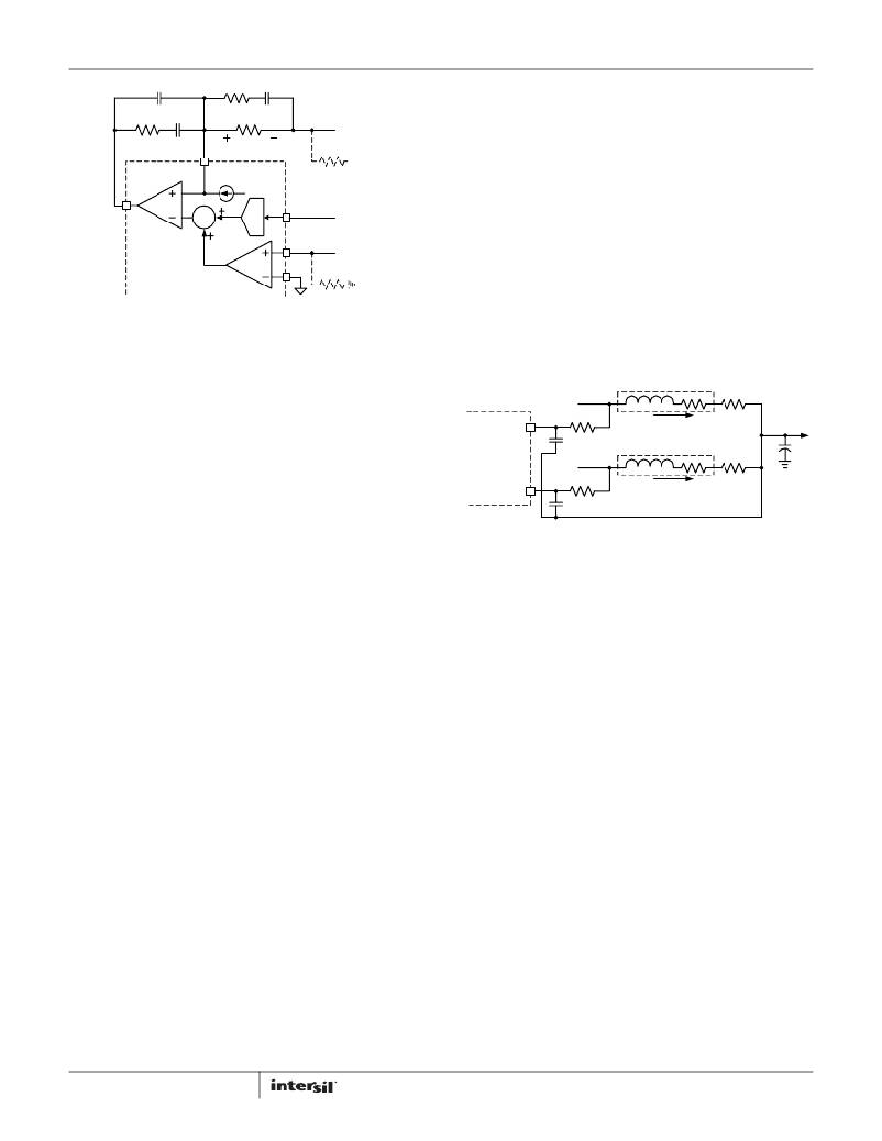
�The� VCC� SENSE� and� VSS� SENSE� signals� come� from� the� processor� die.�
�The� feedback� will� be� open� circuit� in� the� absence� of� the� processor.� As�
�Figure� 12� shows,� it� is� recommended� to� add� a� “catch”� resistor� to� feed�
�the� VR� local� output� voltage� back� to� the� compensator,� and� add�
�another� “catch”� resistor� to� connect� the� VR� local� output� ground� to� the�
�RTN� pin.� These� resistors,� typically� 10� Ω� ~100� Ω� ,� will� provide� voltage�
�FIGURE� 12.� DIFFERENTIAL� SENSING� AND� LOAD� LINE�
�IMPLEMENTATION�
�feedback� if� the� system� is� powered� up� without� a� processor� installed.�
�Phase� Current� Balancing�
�As� the� load� current� increases� from� zero,� the� output� voltage� will�
�droop� from� the� VID� table� value� by� an� amount� proportional� to� the�
�load� current� to� achieve� the� load� line.� The� ISL62882� can� sense�
�the� inductor� current� through� the� intrinsic� DC� Resistance� (DCR)� of�
�the� inductors� as� shown� in� Figure� 1� or� through� resistors� in� series�
�with� the� inductors� as� shown� in� Figure� 2.� In� both� methods,�
�capacitor� C� n� voltage� represents� the� inductor� total� currents.� A�
�droop� amplifier� converts� C� n� voltage� into� an� internal� current�
�source� with� the� gain� set� by� resistor� R� i� .� The� current� source� is� used�
�for� load� line� implementation,� current� monitor� and� overcurrent�
�ISEN2�
�INTERNAL� TO� IC�
�ISEN1�
�PHASE2�
�CS�
�PHASE1�
�CS�
�RS�
�RS�
�L2�
�L1�
�IL2�
�IL1�
�RDCR2�
�RDCR1�
�RPCB2�
�RPCB1�
�VO�
�R� i�
�protection.�
�Figure� 12� shows� the� load� line� implementation.� The� ISL62882�
�drives� a� current� source� I� droop� out� of� the� FB� pin,� described� by�
�Equation� 1.�
�2xV� Cn� (EQ.� 1)�
�I� droop� =� ----------------�
�When� using� inductor� DCR� current� sensing,� a� single� NTC� element�
�is� used� to� compensate� the� positive� temperature� coefficient� of� the�
�FIGURE� 13.� CURRENT� BALANCING� CIRCUIT�
�The� ISL62882� monitors� individual� phase� average� current� by�
�monitoring� the� ISEN1� and� ISEN2� voltages.� Figure� 13� shows� the�
�current� balancing� circuit� recommended� for� ISL62882.� Each�
�phase� node� voltage� is� averaged� by� a� low-pass� filter� consisting� of�
�R� s� and� C� s� ,� and� presented� to� the� corresponding� ISEN� pin.� R� s�
�should� be� routed� to� inductor� phase-node� pad� in� order� to�
�eliminate� the� effect� of� phase� node� parasitic� PCB� DCR.� Equations�
�5� and� 6� give� the� ISEN� pin� voltages:�
�copper� winding� thus� sustaining� the� load� line� accuracy� with�
�reduced� cost.�
�I� droop� flows� through� resistor� R� droop� and� creates� a� voltage� drop� as�
�shown� in� Equation� 2.�
�V� ISEN1� =� (� R� dcr1� +� R� pcb1� )� � I� L1�
�V� ISEN2� =� (� R� dcr2� +� R� pcb2� )� � I� L2�
�(EQ.� 5)�
�(EQ.� 6)�
�V� droop� =� R� droop� � I� droop�
�(EQ.� 2)�
�where� R� dcr1� and� R� dcr2� are� inductor� DCR;� R� pcb1� and� R� pcb2� are�
�parasitic� PCB� DCR� between� the� inductor� output� side� pad� and� the�
�V� droop� is� the� droop� voltage� required� to� implement� load� line.�
�Changing� R� droop� or� scaling� I� droop� can� both� change� the� load� line�
�slope.� Since� I� droop� also� sets� the� overcurrent� protection� level,� it� is�
�recommended� to� first� scale� I� droop� based� on� OCP� requirement,�
�then� select� an� appropriate� R� droop� value� to� obtain� the� desired�
�load� line� slope.�
�Differential� Sensing�
�Figure� 12� also� shows� the� differential� voltage� sensing� scheme.�
�VCC� SENSE� and� VSS� SENSE� are� the� remote� voltage� sensing� signals�
�from� the� processor� die.� A� unity� gain� differential� amplifier� senses�
�the� VSS� SENSE� voltage� and� add� it� to� the� DAC� output.� The� error�
�amplifier� regulates� the� inverting� and� the� non-inverting� input�
�voltages� to� be� equal� as� shown� in� Equation� 3:�
�16�
�output� voltage� rail;� and� I� L1� and� I� L2� are� inductor� average� currents.�
�The� ISL62882� will� adjust� the� phase� pulse-width� relative� to� the�
�other� phase� to� make� V� ISEN1� =� V� ISEN2� ,� thus� to� achieve� I� L1� =� I� L2� ,�
�when� there� are� R� dcr1� =� R� dcr2� and� R� pcb1� =� R� pcb2� .�
�Using� same� components� for� L1� and� L2� will� provide� a� good� match�
�of� R� dcr1� and� R� dcr2� .� Board� layout� will� determine� R� pcb1� and� R� pcb2� .�
�It� is� recommended� to� have� symmetrical� layout� for� the� power�
�delivery� path� between� each� inductor� and� the� output� voltage� rail,�
�such� that� R� pcb1� =� R� pcb2� .�
�FN6890.4�
�June� 21,� 2011�
�相关PDF资料 |
PDF描述 |
|---|---|
| 2512-103K | INDUCTOR POWER 10UH MOLDED SMD |
| ISL6260CCRZ-T | IC REG PWM MULTI-PHASE 40-QFN |
| ESM22DKKN | CONN EDGECARD 44POS .156 WW |
| UPM1C331MPD | CAP ALUM 330UF 16V 20% RADIAL |
| EL5525IREZ-T7 | IC VREF GEN 18CH TFTLCD 38HTSSOP |
相关代理商/技术参数 |
参数描述 |
|---|---|
| ISL62882CEVAL2Z | 功能描述:EVAL BOARD FOR ISL62882C RoHS:是 类别:编程器,开发系统 >> 评估板 - DC/DC 与 AC/DC(离线)SMPS 系列:- 产品培训模块:Obsolescence Mitigation Program 标准包装:1 系列:True Shutdown™ 主要目的:DC/DC,步升 输出及类型:1,非隔离 功率 - 输出:- 输出电压:- 电流 - 输出:1A 输入电压:2.5 V ~ 5.5 V 稳压器拓扑结构:升压 频率 - 开关:3MHz 板类型:完全填充 已供物品:板 已用 IC / 零件:MAX8969 |
| ISL62882CHRTZ | 功能描述:电流型 PWM 控制器 2 PHS PWM BUCKG FOR MICROPROC PWR SUP RoHS:否 制造商:Texas Instruments 开关频率:27 KHz 上升时间: 下降时间: 工作电源电压:6 V to 15 V 工作电源电流:1.5 mA 输出端数量:1 最大工作温度:+ 105 C 安装风格:SMD/SMT 封装 / 箱体:TSSOP-14 |
| ISL62882CHRTZ-T | 功能描述:电流型 PWM 控制器 2 PHS PWM BUCKG FOR MICROPROC PWR SUP RoHS:否 制造商:Texas Instruments 开关频率:27 KHz 上升时间: 下降时间: 工作电源电压:6 V to 15 V 工作电源电流:1.5 mA 输出端数量:1 最大工作温度:+ 105 C 安装风格:SMD/SMT 封装 / 箱体:TSSOP-14 |
| ISL62882CIRTZ | 功能描述:电流型 PWM 控制器 2 PHS PWM BUCKG FOR MICROPROC PWR SUP RoHS:否 制造商:Texas Instruments 开关频率:27 KHz 上升时间: 下降时间: 工作电源电压:6 V to 15 V 工作电源电流:1.5 mA 输出端数量:1 最大工作温度:+ 105 C 安装风格:SMD/SMT 封装 / 箱体:TSSOP-14 |
| ISL62882CIRTZ-T | 功能描述:电流型 PWM 控制器 2 PHS PWM BUCKG FOR MICROPROC PWR SUP RoHS:否 制造商:Texas Instruments 开关频率:27 KHz 上升时间: 下降时间: 工作电源电压:6 V to 15 V 工作电源电流:1.5 mA 输出端数量:1 最大工作温度:+ 105 C 安装风格:SMD/SMT 封装 / 箱体:TSSOP-14 |
发布紧急采购,3分钟左右您将得到回复。