参数资料
| 型号: | ISL6314IRZ |
| 厂商: | Intersil |
| 文件页数: | 28/32页 |
| 文件大小: | 0K |
| 描述: | IC CTRLR PWM 1PHASE BUCK 32-QFN |
| 产品培训模块: | Solutions for Industrial Control Applications |
| 标准包装: | 60 |
| 应用: | 控制器,Intel VR11,AMD CPU |
| 输入电压: | 5 V ~ 12 V |
| 输出数: | 1 |
| 输出电压: | 0.38 V ~ 1.6 V |
| 工作温度: | -40°C ~ 85°C |
| 安装类型: | 表面贴装 |
| 封装/外壳: | 32-VFQFN 裸露焊盘 |
| 供应商设备封装: | 32-QFN 裸露焊盘(5x5) |
| 包装: | 管件 |
第1页第2页第3页第4页第5页第6页第7页第8页第9页第10页第11页第12页第13页第14页第15页第16页第17页第18页第19页第20页第21页第22页第23页第24页第25页第26页第27页当前第28页第29页第30页第31页第32页
�� �
�
�ISL6314�
�C� 2�
�In� high-speed� converters,� the� output� capacitor� bank� is� usually�
�the� most� costly� (and� often� the� largest)� part� of� the� circuit.�
�Output� filter� design� begins� with� minimizing� the� cost� of� this� part�
�R� C�
�C� C�
�COMP�
�of� the� circuit.� The� critical� load� parameters� in� choosing� the�
�output� capacitors� are� the� maximum� size� of� the� load� step,� Δ� I,�
�the� load-current� slew� rate,� di/dt,� and� the� maximum� allowable�
�C� 1�
�R� 1�
�R� FB�
�FB�
�ISL6314�
�output-voltage� deviation� under� transient� loading,� Δ� V� MAX� .�
�Capacitors� are� characterized� according� to� their� capacitance,�
�ESR,� and� ESL� (equivalent� series� inductance).�
�At� the� beginning� of� the� load� transient,� the� output� capacitors�
�VDIFF�
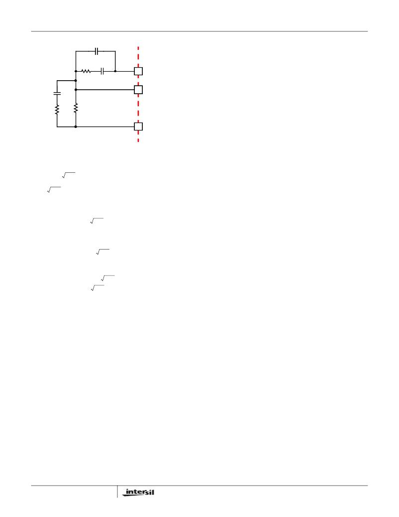
�FIGURE� 21.� COMPENSATION� CIRCUIT� WITHOUT� LOAD-LINE�
�REGULATION�
�supply� all� of� the� transient� current.� The� output� voltage� will�
�initially� deviate� by� an� amount� approximated� by� the� voltage�
�drop� across� the� ESL.� As� the� load� current� increases,� the�
�voltage� drop� across� the� ESR� increases� linearly� until� the� load�
�current� reaches� its� final� value.� The� capacitors� selected� must�
�R� 1� =� R� FB� ?� --------------------------------------------�
�C� 1� =� --------------------------------------------�
�C� 2� =� -----------------------------------------------------------------------------------------------------�
�HF� ?� (� L� ?� C� )� ?� R� FB� ?� V� P-P�
�(� 2� ?� π� )� 2� ?� f� ?� f�
�(EQ.� 38)�
�Δ� V� ≈� ESL� ?� -----� +� ESR� ?� Δ� I�
�.�
�C� ?� ESR�
�L� ?� C� –� C� ?� ESR�
�L� ?� C� –� C� ?� ESR�
�R� FB�
�V� IN�
�0�
�have� sufficiently� low� ESL� and� ESR� so� that� the� total�
�output-voltage� deviation� is� less� than� the� allowable� maximum.�
�Neglecting� the� contribution� of� inductor� current� and� regulator�
�response,� Equation� 38� shows� the� output� voltage� initially�
�deviates� by� an� amount� as� expressed� in� Equation� 38:�
�di�
�dt�
�The� filter� capacitor� must� have� sufficiently� low� ESL� and� ESR�
�V� PP� ?� ?� 2� π� ?� ?� f� 0� ?� f� HF� ?� L� ?� C� ?� R� FB�
�R� C� =� -----------------------------------------------------------------------------------------�
�2�
�?� ?�
�V� IN� ?� (� 2� ?� π� ?� f� HF� ?� L� ?� C� –� 1� )�
�(EQ.� 37)�
�so� that� Δ� V� <� Δ� V� MAX� .�
�Most� capacitor� solutions� rely� on� a� mixture� of� high� frequency�
�capacitors� with� relatively� low� capacitance� in� combination�
�with� bulk� capacitors� having� high� capacitance� but� limited�
�high-frequency� performance.� Minimizing� the� ESL� of� the�
�(� 2� ?� π� )� 2� ?� f� 0� ?� f� HF� ?� (� L� ?� C� )� ?� R� FB� ?� V� P-P�
�V� IN� ?� (� 2� ?� π� ?� f� HF� ?� L� ?� C� –� 1� )�
�C� C� =� -----------------------------------------------------------------------------------------------------�
�In� the� solutions� to� the� compensation� equations,� there� is� a�
�single� degree� of� freedom.� For� the� solutions� presented� in�
�Equation� 37,� R� FB� is� selected� arbitrarily,� typically� in� the� 1k� Ω�
�to� 5k� Ω� range.� The� remaining� compensation� components� are�
�then� selected� according� to� Equation� 37.�
�In� Equation� 37,� L� is� the� filter� inductance;� C� is� the� sum� total� of�
�all� output� capacitors;� ESR� is� the� equivalent-series� resistance�
�of� the� bulk� output-filter� capacitance;� and� V� P-P� is� the�
�peak-to-peak� sawtooth� signal� amplitude� as� described� in� the�
�high-frequency� capacitors� allows� them� to� support� the� output�
�voltage� as� the� current� increases.� Minimizing� the� ESR� of� the�
�bulk� capacitors� allows� them� to� supply� the� increased� current�
�with� less� output� voltage� deviation.�
�The� ESR� of� the� bulk� capacitors� also� creates� the� majority� of�
�the� output-voltage� ripple.� As� the� bulk� capacitors� sink� and�
���bulk� capacitor� ESR� equal� to� I� C(P-P� )� (ESR).� Thus,� once� the�
�output� capacitors� are� selected,� the� maximum� allowable�
�ripple� voltage,� V� P-P(MAX)� ,� determines� the� lower� limit� on� the�
�inductance.�
�–� V� OUT� ?� ?� V� OUT�
�?� V�
�L� ≥� ESR� ?� ----------------------------------------------------------�
��Output� Filter� Design�
�The� output� inductors� and� the� output� capacitor� bank� together�
�?� IN� ?�
�f� S� ?� V� IN� ?� V� P-P� (� MAX� )�
�(EQ.� 39)�
�to� form� a� low-pass� filter� responsible� for� smoothing� the�
�pulsating� voltage� at� the� phase� node.� The� output� filter� also�
�must� provide� the� transient� energy� until� the� regulator� can�
�respond.� Because� it� has� a� low� bandwidth� compared� to� the�
�switching� frequency,� the� output� filter� limits� the� system�
�transient� response.� The� output� capacitors� must� supply� or�
�sink� load� current� while� the� current� in� the� output� inductor�
�increases� or� decreases� to� meet� the� demand.�
�28�
�Since� the� capacitors� are� supplying� a� decreasing� portion� of�
�the� load� current� while� the� regulator� recovers� from� the�
�transient,� the� capacitor� voltage� becomes� slightly� depleted.�
�The� output� inductor� must� be� capable� of� assuming� the� entire�
�load� current� before� the� output� voltage� decreases� more� than�
�Δ� V� MAX� .� This� places� an� upper� limit� on� inductance.�
�Equation� 40� gives� the� upper� limit� on� L� for� the� cases� when�
�the� trailing� edge� of� the� current� transient� causes� a� greater�
�output-voltage� deviation� than� the� leading� edge.� Equation� 41�
�FN6455.2�
�October� 8,� 2009�
�相关PDF资料 |
PDF描述 |
|---|---|
| ISL6315IRZ | IC REG CTRLR BUCK PWM VM 24-QFN |
| ISL6316IRZ | IC REG CTRLR BUCK PWM VM 40-QFN |
| ISL6322GIRZ-T | IC CTRLR PWM BUCK 48-QFN |
| ISL6322IRZ | IC CTRLR PWM 4PHASE BUCK 48-QFN |
| ISL6323AIRZ | IC PWM CTRLR SYNC BUCK DL 48QFN |
相关代理商/技术参数 |
参数描述 |
|---|---|
| ISL6314IRZ-T | 功能描述:IC CTRLR PWM 1PHASE BUCK 32-QFN RoHS:是 类别:集成电路 (IC) >> PMIC - 稳压器 - 专用型 系列:- 标准包装:43 系列:- 应用:控制器,Intel VR11 输入电压:5 V ~ 12 V 输出数:1 输出电压:0.5 V ~ 1.6 V 工作温度:-40°C ~ 85°C 安装类型:表面贴装 封装/外壳:48-VFQFN 裸露焊盘 供应商设备封装:48-QFN(7x7) 包装:管件 |
| ISL6315CRZ | 功能描述:IC REG CTRLR BUCK PWM VM 24-QFN RoHS:是 类别:集成电路 (IC) >> PMIC - 稳压器 - DC DC 切换控制器 系列:- 产品培训模块:Lead (SnPb) Finish for COTS Obsolescence Mitigation Program 标准包装:2,500 系列:- PWM 型:电流模式 输出数:1 频率 - 最大:275kHz 占空比:50% 电源电压:18 V ~ 110 V 降压:无 升压:无 回扫:无 反相:无 倍增器:无 除法器:无 Cuk:无 隔离:是 工作温度:-40°C ~ 85°C 封装/外壳:8-SOIC(0.154",3.90mm 宽) 包装:带卷 (TR) |
| ISL6315CRZ-T | 功能描述:IC REG CTRLR BUCK PWM VM 24-QFN RoHS:是 类别:集成电路 (IC) >> PMIC - 稳压器 - DC DC 切换控制器 系列:- 产品培训模块:Lead (SnPb) Finish for COTS Obsolescence Mitigation Program 标准包装:2,500 系列:- PWM 型:电流模式 输出数:1 频率 - 最大:275kHz 占空比:50% 电源电压:18 V ~ 110 V 降压:无 升压:无 回扫:无 反相:无 倍增器:无 除法器:无 Cuk:无 隔离:是 工作温度:-40°C ~ 85°C 封装/外壳:8-SOIC(0.154",3.90mm 宽) 包装:带卷 (TR) |
| ISL6315CRZ-TK | 功能描述:IC REG CTRLR BUCK PWM VM 24-QFN RoHS:是 类别:集成电路 (IC) >> PMIC - 稳压器 - DC DC 切换控制器 系列:- 产品培训模块:Lead (SnPb) Finish for COTS Obsolescence Mitigation Program 标准包装:2,500 系列:- PWM 型:电流模式 输出数:1 频率 - 最大:275kHz 占空比:50% 电源电压:18 V ~ 110 V 降压:无 升压:无 回扫:无 反相:无 倍增器:无 除法器:无 Cuk:无 隔离:是 工作温度:-40°C ~ 85°C 封装/外壳:8-SOIC(0.154",3.90mm 宽) 包装:带卷 (TR) |
| ISL6315IRZ | 功能描述:IC REG CTRLR BUCK PWM VM 24-QFN RoHS:是 类别:集成电路 (IC) >> PMIC - 稳压器 - DC DC 切换控制器 系列:- 产品培训模块:Lead (SnPb) Finish for COTS Obsolescence Mitigation Program 标准包装:2,500 系列:- PWM 型:电流模式 输出数:1 频率 - 最大:275kHz 占空比:50% 电源电压:18 V ~ 110 V 降压:无 升压:无 回扫:无 反相:无 倍增器:无 除法器:无 Cuk:无 隔离:是 工作温度:-40°C ~ 85°C 封装/外壳:8-SOIC(0.154",3.90mm 宽) 包装:带卷 (TR) |
发布紧急采购,3分钟左右您将得到回复。