- 您现在的位置:买卖IC网 > PDF目录296253 > ISL6426CB (INTERSIL CORP) Triple 3-Input Positive-NAND Gates 14-SOIC -40 to 85 PDF资料下载
参数资料
| 型号: | ISL6426CB |
| 厂商: | INTERSIL CORP |
| 元件分类: | 稳压器 |
| 英文描述: | Triple 3-Input Positive-NAND Gates 14-SOIC -40 to 85 |
| 中文描述: | SWITCHING CONTROLLER, 770 kHz SWITCHING FREQ-MAX, PDSO16 |
| 封装: | PLASTIC, MS-012-AC, SOIC-16 |
| 文件页数: | 2/18页 |
| 文件大小: | 541K |
| 代理商: | ISL6426CB |
10
where IOCSET is the internal OCSET current source (20A
typical). The OC trip point varies mainly due to the MOSFET
rDS(ON) variations. To avoid overcurrent tripping in the
normal operating load range, find the ROCSET resistor from
the equation above with:
1. The maximum rDS(ON) at the highest junction
temperature.
2. The minimum IOCSET from the specification table.
3. Determine IPEAK for, IPEAK > IOUT(MAX) + (DI/2)
where DI is the output inductor ripple current.
For an equation for the ripple current see the section under
Component Selection Guidelines titled Output Inductor
Selection. A small ceramic capacitor should be placed in
parallel with ROCSET to smooth the voltage across ROCSET
in the presence of switching noise on the input voltage.
Current Sinking
The ISL6406, ISL6426 incorporates a MOSFET shoot-
through protection method which allows a converter to sink
current as well as source current. Care should be exercised
when designing a converter with the ISL6406, ISL6426 when
it is known that the converter may sink current. When the
converter is sinking current, it is behaving as a boost
converter that is regulating its input voltage. This means that
the converter is boosting current into the input rail of the
regulator. If there is nowhere for this current to go, such as to
other distributed loads on the rail or through a voltage
limiting protection device, the capacitance on this rail will
absorb the current. This situation will allow the voltage level
of the input rail to increase. If the voltage level of the rail is
boosted to a level that exceeds the maximum voltage rating
of any components attached to the input rail, then those
components may experience an irreversible failure or
experience stress that may shorten their lifespan. Ensuring
that there is a path for the current to flow other than the
capacitance on the rail will prevent this failure mode.
Application Guidelines
Layout Considerations
Layout is very important in high frequency switching
converter design. With power devices switching, the
resulting current transitions from one device to another
cause voltage spikes across the interconnecting
impedances and parasitic circuit elements. These voltage
spikes can degrade efficiency, radiate noise into the circuit,
and lead to device overvoltage stress.
Careful component layout and printed circuit board design
minimizes the voltage spikes in the converters. As an example,
consider the turn-off transition of the PWM MOSFET. Prior to
turn-off, the MOSFET is carrying the full load current. During
turn-off, current stops flowing in the MOSFET and is picked up
by the lower MOSFET. Any parasitic inductance in the switched
current path generates a large voltage spike during the
switching interval. Careful component selection, tight layout of
the critical components, and short, wide traces minimizes the
magnitude of voltage spikes.
There are two sets of critical components in a DC-DC
converter using the ISL6406, ISL6426. The switching
components are the most critical because they switch large
amounts of energy, and therefore tend to generate large
amounts of noise. Next are the small signal components,
which connect to sensitive nodes or supply critical bypass
current and signal coupling.
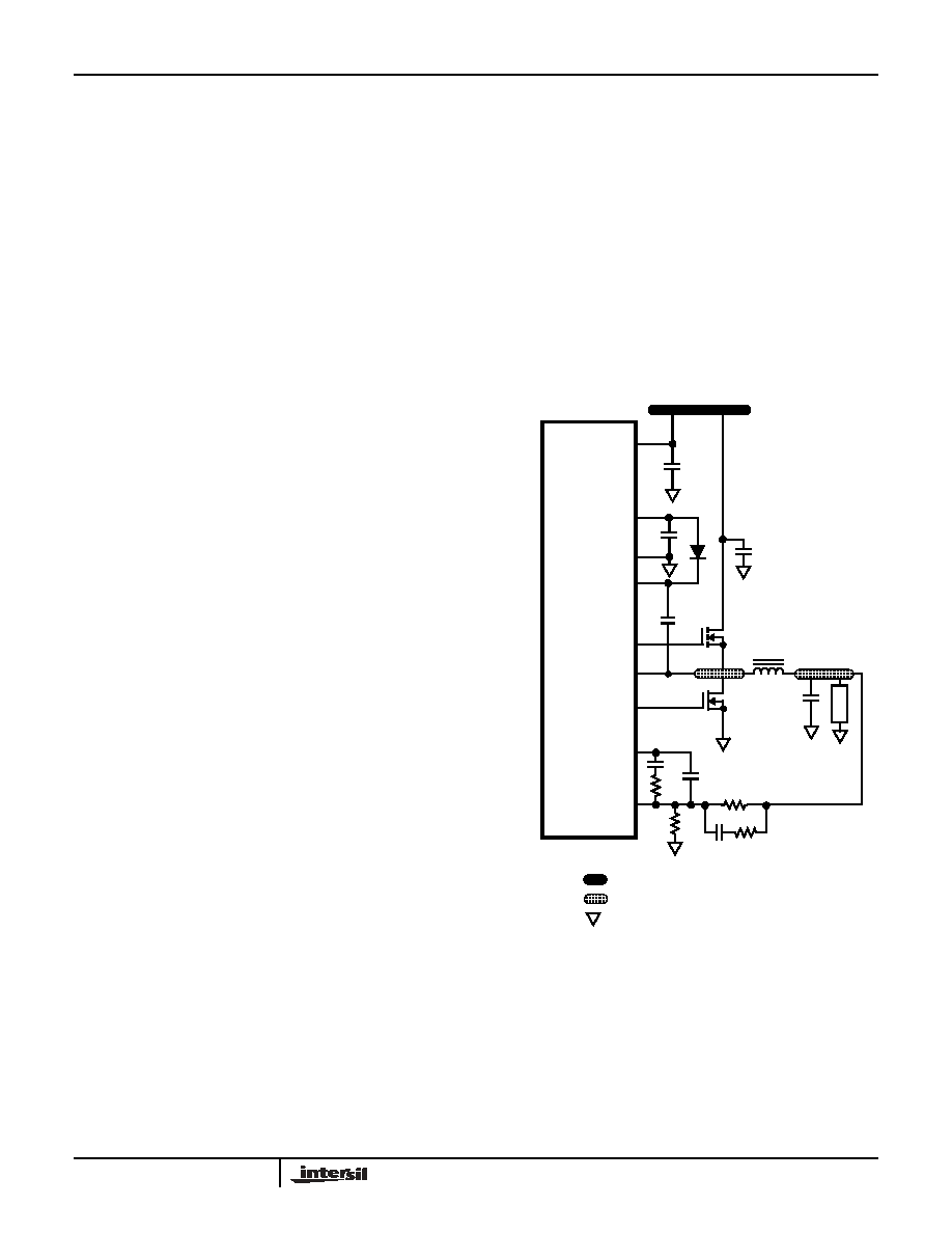
A multi-layer printed circuit board is recommended. Figure 6
shows the connections of the critical components in the
converter. Note that capacitors CIN and COUT could each
represent numerous physical capacitors.
Dedicate one solid layer, usually a middle layer of the PC
board, for a ground plane and make all critical component
ground connections with vias to this layer. Dedicate another
solid layer as a power plane and break this plane into
smaller islands of common voltage levels. Keep the metal
runs from the PHASE terminals to the output inductor short.
The power plane should support the input power and output
VOUT
ISLAND ON POWER PLANE LAYER
ISLAND ON CIRCUIT PLANE LAYER
LOUT
COUT
CIN
+3.3V VIN
KEY
COMP
ISL6406
UGATE
R4
R2
CBP
FB
GND
CPVOUT
FIGURE 6. PRINTED CIRCUIT BOARD POWER PLANES
AND ISLANDS
R1
BOOT
C2
VIA CONNECTION TO GROUND PLANE
LO
AD
Q1
CBOOT
PHASE
D1
R3
C3
C1
Q2
LGATE
PHASE
VCC
CVCC
ISL6406, ISL6426
相关PDF资料 |
PDF描述 |
|---|---|
| ISL6426CBZ | Single Synchronous Buck Pulse-Width Modulation (PWM) Controller |
| ISL6426CR | Single Synchronous Buck Pulse-Width Modulation (PWM) Controller |
| ISL6426CRZ | Single Synchronous Buck Pulse-Width Modulation (PWM) Controller |
| ISL6426CRZ-T | Single Synchronous Buck Pulse-Width Modulation (PWM) Controller |
| ISL6426CV | Single Synchronous Buck Pulse-Width Modulation (PWM) Controller |
相关代理商/技术参数 |
参数描述 |
|---|---|
| ISL6426CR | 制造商:Rochester Electronics LLC 功能描述:- Bulk 制造商:Intersil Corporation 功能描述: |
| ISL6426CV | 制造商:Rochester Electronics LLC 功能描述:- Bulk 制造商:Intersil Corporation 功能描述: |
| ISL6426IB | 制造商:Rochester Electronics LLC 功能描述:- Bulk |
| ISL6426IB-T | 制造商:Rochester Electronics LLC 功能描述:- Tape and Reel |
| ISL6426IR | 制造商:Rochester Electronics LLC 功能描述:- Bulk |
发布紧急采购,3分钟左右您将得到回复。