- 您现在的位置:买卖IC网 > PDF目录16715 > ISL6505CRZ (Intersil)IC PWR SUPPLY CTRLR/MONITR 20QFN PDF资料下载
参数资料
| 型号: | ISL6505CRZ |
| 厂商: | Intersil |
| 文件页数: | 8/17页 |
| 文件大小: | 0K |
| 描述: | IC PWR SUPPLY CTRLR/MONITR 20QFN |
| 标准包装: | 60 |
| 应用: | 电源控制器/监控器 |
| 电源电压: | 4.75 V ~ 5.25 V |
| 电流 - 电源: | 6mA |
| 工作温度: | 0°C ~ 70°C |
| 安装类型: | 表面贴装 |
| 封装/外壳: | 20-VQFN 裸露焊盘 |
| 供应商设备封装: | 20-QFN 裸露焊盘(5x5) |
| 包装: | 管件 |
�� �
�
�ISL6505�
�The� internal� circuitry� does� not� allow� the� transition� from� an�
�S4/S5� (suspend� to� disk/soft� off)� state� to� an� S3� (suspend� to�
�RAM)� state;� however,� it� does� allow� the� transition� from� S3� to�
�S4/S5.� The� only� ‘legal’� transitions� are� from� an� active� state�
�(S0,� S1)� to� a� sleep� state� (S3,� S5)� and� vice� versa.�
�TABLE� 1.� 5V� DUAL� OUTPUT� (V� OUT4� )� AND� 3.3VDL/SB� (V� OUT3� )�
�TRUTH� TABLE�
�5VSB�
�S3�
�S5�
�3.3V,� 5V�
�S5�
�1�
�1�
�0�
�S3�
�1�
�0�
�1�
�3.3VDL/SB�
�3.3V�
�3.3V�
�Note�
�5VDL�
�5V�
�5V�
�COMMENTS�
�S0/S1/S2� States� (Active)�
�S3�
�Maintains� Previous� State�
�3V3DLSB�
�DLA�
�3V3DL�
�5VDLSB�
�0�
�0�
�3.3V�
�0V�
�S4/S5� (EN5� =� GND)�
�0�
�0�
�3.3V�
�5V�
�S4/S5� (EN5� =� open/5V)�
�5VDL�
�NOTE:� Combination� Not� Allowed.�
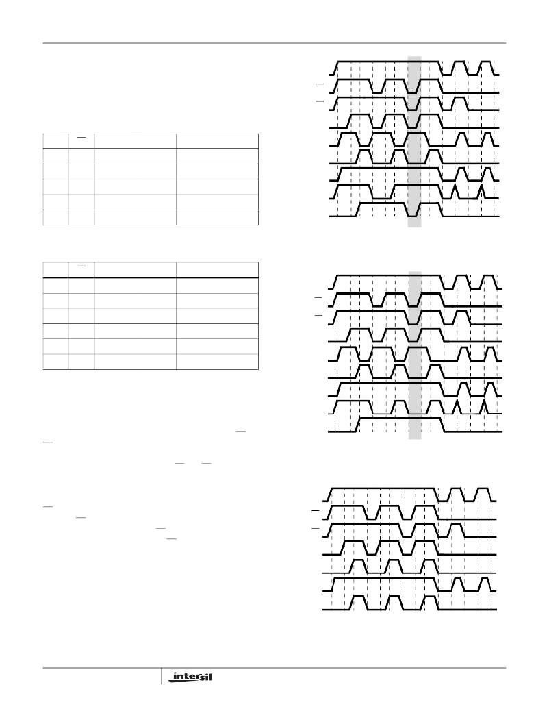
�FIGURE� 4.� 5V� DUAL� AND� 3.3V� DUAL� /3.3V� SB� TIMING�
�DIAGRAM;� EN5� =� GND�
�TABLE� 2.� V� OUT1� AND� 1V2VID� (V� OUT2� )� TRUTH� TABLE�
�S5�
�S3�
�V� OUT1�
�1V2VID�
�COMMENTS�
�1�
�1�
�1�
�0�
�0�
�0�
�1�
�0�
�0�
�1�
�0�
�0�
�1.5V�
�0V�
�1.5V�
�0V�
�1.5V�
�Note�
�1.2V�
�0V�
�0V�
�0V�
�0V�
�S0/S1/S2� States� (Active)�
�S3� (LAN� =� GND)�
�S3� (LAN� =� open/5V)�
�Maintains� Previous� State�
�S4/S5� (LAN� =� GND)�
�S4/S5� (LAN� =� open/5V)�
�5VSB�
�S3�
�S5�
�3.3V,� 5V�
�3V3DLSB�
�NOTE:� Combination� Not� Allowed.�
�DLA�
�3V3DL�
�Functional� Timing� Diagrams�
�Figures� 4� (EN5� =� low),� 5� (EN5� =� high),� and� 6� are� timing�
�diagrams,� detailing� the� power� up/down� sequences� of� all� the�
�outputs� in� response� to� the� status� of� the� sleep-state� pins� (S3,�
�S5),� as� well� as� the� status� of� the� input� ATX� supply.� Not� shown� in�
�these� diagrams� is� the� deglitching� feature� used� to� protect�
�against� false� sleep� state� tripping.� Both� S3� and� S5� pins� are�
�protected� against� noise� by� a� 2μs� filter� (typically� 1–4� μ� s).� This�
�feature� is� useful� in� noisy� computer� environments� if� the� control�
�signals� have� to� travel� over� significant� distances.� Additionally,� the�
�S3� pin� features� a� 200� μ� s� delay� in� transitioning� to� sleep� states.�
�Once� the� S3� pin� goes� low,� an� internal� timer� is� activated.� At� the�
�end� of� the� 200μs� interval,� if� the� S5� pin� is� low,� the� ISL6505�
�switches� into� S5� sleep� state;� if� the� S5� pin� is� high,� the�
�ISL6505� goes� into� S3� sleep� state.�
�The� shaded� column� in� Figures� 4� and� 5� highlights� the�
�difference� on� the� 5VDLSB� and� 5VDL� pins� for� the� two� EN5�
�states.�
�5VDLSB�
�5VDL�
�FIGURE� 5.� 5V� DUAL� AND� 3.3V� DUAL� /3.3V� SB� TIMING�
�DIAGRAM;� EN5� =� 5V/OPEN�
�5VSB�
�S3�
�S5�
�3.3V,�
�5V,� 12V�
�DLA�
�V� OUT1�
�(LAN=5V)�
�1V2VID�
�V� OUT1� (LAN=GND)�
�FIGURE� 6.� V� OUT1� AND� 1.2V� VID� TIMING� DIAGRAM� (NOTE�
�THE� DEPENDENCE� OF� V� OUT1� ON� THE� LOGIC�
�STATE� OF� LAN� PIN)�
�8�
�相关PDF资料 |
PDF描述 |
|---|---|
| RBM12DTKD-S288 | CONN EDGECARD 24POS .156 EXTEND |
| ISL62383CHRTZ | IC PWR SUPPLY CONTROLLER 28TQFN |
| RBM06DRMT-S288 | CONN EDGECARD 12POS .156 EXTEND |
| GMM12DTKN-S288 | CONN EDGECARD 24POS .156 EXTEND |
| V72B3V3E100BL2 | CONVERTER MOD DC/DC 3.3V 100W |
相关代理商/技术参数 |
参数描述 |
|---|---|
| ISL6505CRZ-T | 功能描述:IC PWR SUPPLY CTRLR/MONITR 20QFN RoHS:是 类别:集成电路 (IC) >> PMIC - 电源控制器,监视器 系列:- 产品培训模块:Lead (SnPb) Finish for COTS Obsolescence Mitigation Program 标准包装:2,500 系列:- 应用:多相控制器 输入电压:- 电源电压:9 V ~ 14 V 电流 - 电源:- 工作温度:-40°C ~ 85°C 安装类型:表面贴装 封装/外壳:40-WFQFN 裸露焊盘 供应商设备封装:40-TQFN-EP(5x5) 包装:带卷 (TR) |
| ISL6506ACB | 功能描述:IC MULTIPLE POWER CTRLR 8LEPSOIC RoHS:否 类别:集成电路 (IC) >> PMIC - 电源控制器,监视器 系列:- 产品培训模块:Lead (SnPb) Finish for COTS Obsolescence Mitigation Program 标准包装:2,500 系列:- 应用:多相控制器 输入电压:- 电源电压:9 V ~ 14 V 电流 - 电源:- 工作温度:-40°C ~ 85°C 安装类型:表面贴装 封装/外壳:40-WFQFN 裸露焊盘 供应商设备封装:40-TQFN-EP(5x5) 包装:带卷 (TR) |
| ISL6506ACB-T | 功能描述:IC MULTIPLE POWER CTRLR 8LEPSOIC RoHS:否 类别:集成电路 (IC) >> PMIC - 电源控制器,监视器 系列:- 产品培训模块:Lead (SnPb) Finish for COTS Obsolescence Mitigation Program 标准包装:2,500 系列:- 应用:多相控制器 输入电压:- 电源电压:9 V ~ 14 V 电流 - 电源:- 工作温度:-40°C ~ 85°C 安装类型:表面贴装 封装/外壳:40-WFQFN 裸露焊盘 供应商设备封装:40-TQFN-EP(5x5) 包装:带卷 (TR) |
| ISL6506ACBZ | 功能描述:DC/DC 开关控制器 2 OUTPUT ACPI PWR CNTRLR 8LD EP RoHS:否 制造商:Texas Instruments 输入电压:6 V to 100 V 开关频率: 输出电压:1.215 V to 80 V 输出电流:3.5 A 输出端数量:1 最大工作温度:+ 125 C 安装风格: 封装 / 箱体:CPAK |
| ISL6506ACBZ-T | 功能描述:DC/DC 开关控制器 ISL6506A 2 OUTPUT ACPI CNTRLR 8L EP RoHS:否 制造商:Texas Instruments 输入电压:6 V to 100 V 开关频率: 输出电压:1.215 V to 80 V 输出电流:3.5 A 输出端数量:1 最大工作温度:+ 125 C 安装风格: 封装 / 箱体:CPAK |
发布紧急采购,3分钟左右您将得到回复。