- 您现在的位置:买卖IC网 > PDF目录15084 > ISL6520ACB-T (Intersil)IC REG CTRLR BUCK PWM VM 8-SOIC PDF资料下载
参数资料
| 型号: | ISL6520ACB-T |
| 厂商: | Intersil |
| 文件页数: | 8/12页 |
| 文件大小: | 0K |
| 描述: | IC REG CTRLR BUCK PWM VM 8-SOIC |
| 标准包装: | 1 |
| PWM 型: | 电压模式 |
| 输出数: | 1 |
| 频率 - 最大: | 340kHz |
| 占空比: | 100% |
| 电源电压: | 4.5 V ~ 5.5 V |
| 降压: | 是 |
| 升压: | 无 |
| 回扫: | 无 |
| 反相: | 无 |
| 倍增器: | 无 |
| 除法器: | 无 |
| Cuk: | 无 |
| 隔离: | 无 |
| 工作温度: | 0°C ~ 70°C |
| 封装/外壳: | 8-SOIC(0.154",3.90mm 宽) |
| 包装: | 标准包装 |
| 其它名称: | ISL6520ACB-DKR ISL6520ACB-DKR-ND ISL6520ACBDKR |
�� �
�
�ISL6520A�
�F� Z1� =� ------------------------------------�
�F� P1� =� ---------------------------------------------------------�
�2� π� x� R� 2� x� ?� ----------------------� ?�
�4.� Place� 1� ST� Pole� at� the� ESR� Zero.�
�5.� Place� 2� ND� Pole� at� Half� the� Switching� Frequency.�
�6.� Check� Gain� against� Error� Amplifier� ’s� Open-Loop� Gain.�
�7.� Estimate� Phase� Margin� -� Repeat� if� Necessary.�
�Compensation� Break� Frequency� Equations�
�1� 1�
�2� π� x� R� 2� x� C� 1� ?� C� 1� x� C� 2� ?�
�?� C� 1� +� C� 2� ?�
�These� requirements� are� generally� met� with� a� mix� of�
�capacitors� and� careful� layout.�
�Modern� components� and� loads� are� capable� of� producing�
�transient� load� rates� above� 1A/ns.� High� frequency� capacitors�
�initially� supply� the� transient� and� slow� the� current� load� rate�
�seen� by� the� bulk� capacitors.� The� bulk� filter� capacitor� values�
�are� generally� determined� by� the� ESR� (Effective� Series�
�Resistance)� and� voltage� rating� requirements� rather� than�
�actual� capacitance� requirements.�
�F� Z2� =� -------------------------------------------------------�
�F� P2� =� ------------------------------------�
�1�
�2� π� x� (� R� 1� +� R� 3� )� x� C� 3�
�1�
�2� π� x� R� 3� x� C� 3�
�(EQ.� 5)�
�High� frequency� decoupling� capacitors� should� be� placed� as�
�close� to� the� power� pins� of� the� load� as� physically� possible.� Be�
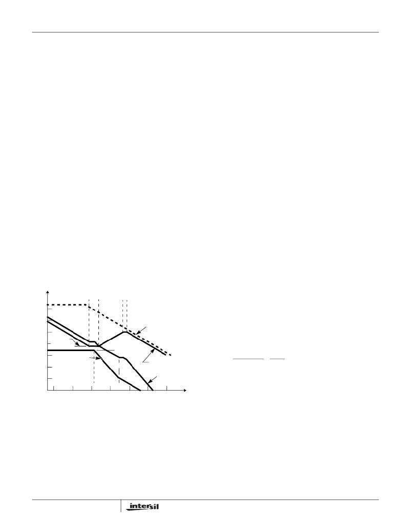
�Figure� 6� shows� an� asymptotic� plot� of� the� DC/DC� converter’s�
�gain� vs� frequency.� The� actual� Modulator� Gain� has� a� high� gain�
�peak� due� to� the� high� Q� factor� of� the� output� filter� and� is� not�
�shown� in� Figure� 6.� Using� the� previously� mentioned� guidelines�
�should� give� a� Compensation� Gain� similar� to� the� curve� plotted.�
�The� open� loop� error� amplifier� gain� bounds� the� compensation�
�gain.� Check� the� compensation� gain� at� F� P2� with� the�
�capabilities� of� the� error� amplifier.� The� Closed� Loop� Gain� is�
�constructed� on� the� graph� of� Figure� 6� by� adding� the� Modulator�
�Gain� (in� dB)� to� the� Compensation� Gain� (in� dB).� This� is�
�equivalent� to� multiplying� the� modulator� transfer� function� to� the�
�compensation� transfer� function� and� plotting� the� gain.�
�The� compensation� gain� uses� external� impedance� networks�
�Z� FB� and� Z� IN� to� provide� a� stable,� high� bandwidth� (BW)� overall�
�loop.� A� stable� control� loop� has� a� gain� crossing� with�
�-20dB/decade� slope� and� a� phase� margin� greater� than� 45�
�degrees.� Include� worst� case� component� variations� when�
�determining� phase� margin.�
�careful� not� to� add� inductance� in� the� circuit� board� wiring� that�
�could� cancel� the� usefulness� of� these� low� inductance�
�components.� Consult� with� the� manufacturer� of� the� load� on�
�specific� decoupling� requirements.�
�Use� only� specialized� low-ESR� capacitors� intended� for�
�switching-regulator� applications� for� the� bulk� capacitors.� The�
�bulk� capacitor’s� ESR� will� determine� the� output� ripple� voltage�
�and� the� initial� voltage� drop� after� a� high� slew-rate� transient.� An�
�aluminum� electrolytic� capacitor’s� ESR� value� is� related� to� the�
�case� size� with� lower� ESR� available� in� larger� case� sizes.�
�However,� the� Equivalent� Series� Inductance� (ESL)� of� these�
�capacitors� increases� with� case� size� and� can� reduce� the�
�usefulness� of� the� capacitor� to� high� slew-rate� transient� loading.�
�Unfortunately,� ESL� is� not� a� specified� parameter.� Work� with�
�your� capacitor� supplier� and� measure� the� capacitor’s�
�impedance� with� frequency� to� select� a� suitable� component.� In�
�most� cases,� multiple� electrolytic� capacitors� of� small� case� size�
�perform� better� than� a� single� large� case� capacitor.�
�100�
�F� Z1� F� Z2�
�F� P1�
�F� P2�
�Output� Inductor� Selection�
�The� output� inductor� is� selected� to� meet� the� output� voltage�
�80�
�ripple� requirements� and� minimize� the� converter� ’s� response�
�60�
�40�
�20�
�20LOG�
�(R� 2� /R� 1� )�
�OPEN� LOOP�
�ERROR� AMP� GAIN�
�20LOG�
�time� to� the� load� transient.� The� inductor� value� determines� the�
�converter� ’s� ripple� current� and� the� ripple� voltage� is� a� function�
�of� the� ripple� current.� The� ripple� voltage� and� current� are�
�approximated� by� the� following� equations:�
�0�
�-20�
�MODULATOR�
�GAIN�
�(V� IN� /� D� V� OSC� )�
�COMPENSATION�
�GAIN�
�Δ� I� =�
�V� IN� - V� OUT�
�Fs� x� L�
�x�
�V� OUT�
�V� IN�
�Δ� V� OUT� =� Δ� I� x� ESR�
�(EQ.� 6)�
�-40�
�-60�
�10�
�100�
�1K�
�F� LC�
�10K�
�F� ESR�
�100K�
�1M�
�CLOSED� LOOP�
�GAIN�
�10M�
�Increasing� the� value� of� inductance� reduces� the� ripple� current�
�and� voltage.� However,� the� large� inductance� values� reduce�
�the� converter� ’s� response� time� to� a� load� transient.�
�FREQUENCY� (Hz)�
�FIGURE� 6.� ASYMPTOTIC� BODE� PLOT� OF� CONVERTER� GAIN�
�Component� Selection� Guidelines�
�Output� Capacitor� Selection�
�An� output� capacitor� is� required� to� filter� the� output� and� supply�
�the� load� transient� current.� The� filtering� requirements� are� a�
�function� of� the� switching� frequency� and� the� ripple� current.�
�The� load� transient� requirements� are� a� function� of� the� slew�
�rate� (di/dt)� and� the� magnitude� of� the� transient� load� current.�
�8�
�One� of� the� parameters� limiting� the� converter� ’s� response� to�
�a� load� transient� is� the� time� required� to� change� the� inductor�
�current.� Given� a� sufficiently� fast� control� loop� design,� the�
�ISL6520A� will� provide� either� 0%� or� 100%� duty� cycle� in�
�response� to� a� load� transient.� The� response� time� is� the� time�
�required� to� slew� the� inductor� current� from� an� initial� current�
�value� to� the� transient� current� level.� During� this� interval� the�
�difference� between� the� inductor� current� and� the� transient�
�current� level� must� be� supplied� by� the� output� capacitor.�
�Minimizing� the� response� time� can� minimize� the� output�
�capacitance� required.�
�FN9016.6�
�December� 10,� 2009�
�相关PDF资料 |
PDF描述 |
|---|---|
| X4043S8IZ-2.7A | IC CPU SUPERV 4K EEPROM 8-SOIC |
| VI-25X-EW-F3 | CONVERTER MOD DC/DC 5.2V 100W |
| X4043S8IZ-2.7 | IC CPU SUPERV 4K EEPROM 8-SOIC |
| X4043S8IZ | IC CPU SUPERV 4K EEPROM 8-SOIC |
| VI-25W-EW-F4 | CONVERTER MOD DC/DC 5.5V 100W |
相关代理商/技术参数 |
参数描述 |
|---|---|
| ISL6520ACBZ | 功能描述:电压模式 PWM 控制器 VER OF ISL6520ACB RoHS:否 制造商:Texas Instruments 输出端数量:1 拓扑结构:Buck 输出电压:34 V 输出电流: 开关频率: 工作电源电压:4.5 V to 5.5 V 电源电流:600 uA 最大工作温度:+ 125 C 最小工作温度:- 40 C 封装 / 箱体:WSON-8 封装:Reel |
| ISL6520ACBZA | 功能描述:IC REG CTRLR BUCK PWM VM 8-SOIC RoHS:是 类别:集成电路 (IC) >> PMIC - 稳压器 - DC DC 切换控制器 系列:- 产品培训模块:Lead (SnPb) Finish for COTS Obsolescence Mitigation Program 标准包装:2,500 系列:- PWM 型:电流模式 输出数:1 频率 - 最大:275kHz 占空比:50% 电源电压:18 V ~ 110 V 降压:无 升压:无 回扫:无 反相:无 倍增器:无 除法器:无 Cuk:无 隔离:是 工作温度:-40°C ~ 85°C 封装/外壳:8-SOIC(0.154",3.90mm 宽) 包装:带卷 (TR) |
| ISL6520ACBZA-T | 功能描述:IC REG CTRLR BUCK PWM VM 8-SOIC RoHS:是 类别:集成电路 (IC) >> PMIC - 稳压器 - DC DC 切换控制器 系列:- 产品培训模块:Lead (SnPb) Finish for COTS Obsolescence Mitigation Program 标准包装:2,500 系列:- PWM 型:电流模式 输出数:1 频率 - 最大:275kHz 占空比:50% 电源电压:18 V ~ 110 V 降压:无 升压:无 回扫:无 反相:无 倍增器:无 除法器:无 Cuk:无 隔离:是 工作温度:-40°C ~ 85°C 封装/外壳:8-SOIC(0.154",3.90mm 宽) 包装:带卷 (TR) |
| ISL6520ACBZA-TS2490 | 制造商:Rochester Electronics LLC 功能描述: 制造商:Intersil Corporation 功能描述: |
| ISL6520ACBZ-T | 功能描述:电压模式 PWM 控制器 VER OF ISL6520ACB-T RoHS:否 制造商:Texas Instruments 输出端数量:1 拓扑结构:Buck 输出电压:34 V 输出电流: 开关频率: 工作电源电压:4.5 V to 5.5 V 电源电流:600 uA 最大工作温度:+ 125 C 最小工作温度:- 40 C 封装 / 箱体:WSON-8 封装:Reel |
发布紧急采购,3分钟左右您将得到回复。