- 您现在的位置:买卖IC网 > PDF目录15068 > ISL6520IR (Intersil)IC REG CTRLR BUCK PWM VM 16-QFN PDF资料下载
参数资料
| 型号: | ISL6520IR |
| 厂商: | Intersil |
| 文件页数: | 6/11页 |
| 文件大小: | 0K |
| 描述: | IC REG CTRLR BUCK PWM VM 16-QFN |
| 标准包装: | 75 |
| PWM 型: | 电压模式 |
| 输出数: | 1 |
| 频率 - 最大: | 340kHz |
| 占空比: | 100% |
| 电源电压: | 4.5 V ~ 5.5 V |
| 降压: | 是 |
| 升压: | 无 |
| 回扫: | 无 |
| 反相: | 无 |
| 倍增器: | 无 |
| 除法器: | 无 |
| Cuk: | 无 |
| 隔离: | 无 |
| 工作温度: | -40°C ~ 85°C |
| 封装/外壳: | 16-VQFN 裸露焊盘 |
| 包装: | 管件 |
�� �
�
�ISL6520�
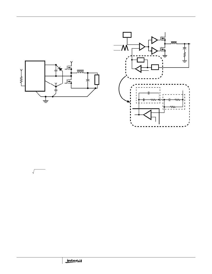
�Figure� 4� shows� the� circuit� traces� that� require� additional� layout�
�consideration.� Use� single� point� and� ground� plane� construction�
�for� the� circuits� shown.� Minimize� any� leakage� current� paths� on�
�7.� Estimate� Phase� Margin� -� Repeat� if� Necessary.�
�the� COMP/OCSET� pin� and� locate� the� resistor,� R� OSCET� close�
�OSC�
�DRIVER�
�V� IN�
�to� the� COMP/OCSET� pin� because� the� internal� current� source� is�
�only� 20� μ� A.� Provide� local� V� CC� decoupling� between� VCC� and�
�GND� pins.� Locate� the� capacitor,� C� BOOT� as� close� as� practical� to�
�Δ� V� OSC�
�PWM�
�COMPARATOR�
�-�
�+�
�DRIVER�
�L� O�
�PHASE�
�C� O�
�V� OUT�
�the� BOOT� and� PHASE� pins.� All� components� used� for� feedback�
�compensation� should� be� located� as� close� to� the� IC� a� practical.�
�ESR�
�+5V�
�ISL6520�
�BOOT�
�C� BOOT�
�PHASE�
�D� 1�
�+V� IN�
�Q� 1�
�L� O�
�V� OUT�
�Z� FB�
�V� E/A�
�-�
�+�
�ERROR�
�AMP�
�Z� IN�
�REFERENCE�
�(PARASITIC)�
�VCC�
�+5V�
�Q� 2�
�C� O�
�DETAILED� COMPENSATION� COMPONENTS�
�COMP/OCSET�
�GND�
�C� VCC�
�C� 1�
�C� 2�
�R� 2�
�Z� FB�
�C� 3�
�Z� IN�
�R� 3�
�V� OUT�
�FIGURE� 4.� PRINTED� CIRCUIT� BOARD� SMALL� SIGNAL�
�LAYOUT� GUIDELINES�
�Feedback� Compensation�
�Figure� 5� highlights� the� voltage-mode� control� loop� for� a�
�synchronous-rectified� buck� converter.� The� output� voltage�
�COMP�
�-�
�+�
�ISL6520�
�REFERENCE�
�FB�
�R� 1�
�(V� OUT� )� is� regulated� to� the� Reference� voltage� level.� The�
�error� amplifier� (Error� Amp)� output� (V� E/A� )� is� compared� with�
�the� oscillator� (OSC)� triangular� wave� to� provide� a� pulse-�
�width� modulated� (PWM)� wave� with� an� amplitude� of� V� IN� at�
�the� PHASE� node.� The� PWM� wave� is� smoothed� by� the� output�
�filter� (L� O� and� C� O� ).�
�Modulator� Break� Frequency� Equations�
�FIGURE� 5.� VOLTAGE-MODE� BUCK� CONVERTER�
�COMPENSATION� DESIGN�
�The� modulator� transfer� function� is� the� small-signal� transfer�
�function� of� V� OUT� /V� E/A� .� This� function� is� dominated� by� a� DC�
�Gain� and� the� output� filter� (L� O� and� C� O� ),� with� a� double� pole�
�break� frequency� at� F� LC� and� a� zero� at� F� ESR� .� The� DC� Gain� of�
�the� modulator� is� simply� the� input� voltage� (V� IN� )� divided� by� the�
�peak-to-peak� oscillator� voltage� Δ� V� OSC� .�
�F� LC� =� -------------------------------------------�
�F� ESR� =� --------------------------------------------�
�1�
�2� π� x� LO� x� CO�
�1�
�2� π� x� ESR� x� C� O�
�Compensation� Break� Frequency� Equations�
�F� Z1� =� ------------------------------------�
�F� P1� =� ---------------------------------------------------------�
�2� π� x� R� 2� x� ?� ----------------------� ?�
�F� Z2� =� -------------------------------------------------------�
�F� P2� =� ------------------------------------�
�(EQ.� 4)�
�The� compensation� network� consists� of� the� error� amplifier�
�(internal� to� the� ISL6520)� and� the� impedance� networks� Z� IN�
�and� Z� FB� .� The� goal� of� the� compensation� network� is� to� provide�
�a� closed� loop� transfer� function� with� the� highest� 0dB� crossing�
�1�
�2� π� x� R� 2� x� C� 1�
�1�
�2� π� x� (� R� 1� +� R� 3� )� x� C� 3�
�1�
�?� C� 1� x� C� 2� ?�
�?� C� 1� +� C� 2� ?�
�1�
�2� π� x� R� 3� x� C� 3�
�frequency� (f� 0dB� )� and� adequate� phase� margin.� Phase� margin�
�is� the� difference� between� the� closed� loop� phase� at� f� 0dB� and�
�180� degrees.� The� equations� below� relate� the� compensation�
�network’s� poles,� zeros� and� gain� to� the� components� (R� 1� ,� R� 2� ,�
�R� 3� ,� C� 1� ,� C� 2� ,� and� C� 3� )� in� Figure� 7.� Use� these� guidelines� for�
�locating� the� poles� and� zeros� of� the� compensation� network:�
�1.� Pick� Gain� (R� 2� /R� 1� )� for� desired� converter� bandwidth.�
�2.� Place� 1� ST� Zero� Below� Filter’s� Double� Pole� (~75%� F� LC� ).�
�3.� Place� 2� ND� Zero� at� Filter� ’s� Double� Pole.�
�4.� Place� 1� ST� Pole� at� the� ESR� Zero.�
�5.� Place� 2� ND� Pole� at� Half� the� Switching� Frequency.�
�6.� Check� Gain� against� Error� Amplifier� ’s� Open-Loop� Gain.�
�6�
�(EQ.� 5)�
�Figure� 6� shows� an� asymptotic� plot� of� the� DC/DC� converter’s�
�gain� vs� frequency.� The� actual� Modulator� Gain� has� a� high� gain�
�peak� due� to� the� high� Q� factor� of� the� output� filter� and� is� not�
�shown� in� Figure� 6.� Using� the� above� guidelines� should� give� a�
�Compensation� Gain� similar� to� the� curve� plotted.� The� open�
�loop� error� amplifier� gain� bounds� the� compensation� gain.�
�Check� the� compensation� gain� at� F� P2� with� the� capabilities� of�
�the� error� amplifier.� The� Closed� Loop� Gain� is� constructed� on�
�the� graph� of� Figure� 6� by� adding� the� Modulator� Gain� (in� dB)� to�
�the� Compensation� Gain� (in� dB).� This� is� equivalent� to�
�multiplying� the� modulator� transfer� function� to� the�
�compensation� transfer� function� and� plotting� the� gain.�
�FN9009.6�
�April� 3,� 2007�
�相关PDF资料 |
PDF描述 |
|---|---|
| RCM43DCMN-S288 | CONN EDGECARD 86POS .156 EXTEND |
| ISL6522IB | IC REG CTRLR BST PWM VM 14-SOIC |
| RCM43DCMH-S288 | CONN EDGECARD 86POS .156 EXTEND |
| ISL6522CV-T | IC REG CTRLR BST PWM VM 14-TSSOP |
| RCM43DCMD-S288 | CONN EDGECARD 86POS .156 EXTEND |
相关代理商/技术参数 |
参数描述 |
|---|---|
| ISL6520IR-T | 功能描述:IC REG CTRLR BUCK PWM VM 16-QFN RoHS:否 类别:集成电路 (IC) >> PMIC - 稳压器 - DC DC 切换控制器 系列:- 标准包装:4,000 系列:- PWM 型:电压模式 输出数:1 频率 - 最大:1.5MHz 占空比:66.7% 电源电压:4.75 V ~ 5.25 V 降压:是 升压:无 回扫:无 反相:无 倍增器:无 除法器:无 Cuk:无 隔离:无 工作温度:-40°C ~ 85°C 封装/外壳:40-VFQFN 裸露焊盘 包装:带卷 (TR) |
| ISL6521CB | 功能描述:IC REG QD BCK/LINEAR 16-SOIC RoHS:否 类别:集成电路 (IC) >> PMIC - 稳压器 - 线性 + 切换式 系列:- 标准包装:2,500 系列:- 拓扑:降压(降压)同步(2),线性(LDO)(1) 功能:任何功能 输出数:3 频率 - 开关:300kHz 电压/电流 - 输出 1:控制器 电压/电流 - 输出 2:控制器 电压/电流 - 输出 3:控制器 带 LED 驱动器:无 带监控器:无 带序列发生器:是 电源电压:4.5 V ~ 24 V 工作温度:-40°C ~ 85°C 安装类型:* 封装/外壳:28-TSSOP(0.173",4.40mm 宽) 供应商设备封装:* 包装:带卷 (TR) 其它名称:ISL6402IVZ-TTR |
| ISL6521CB-T | 功能描述:IC REG QD BCK/LINEAR 16-SOIC RoHS:否 类别:集成电路 (IC) >> PMIC - 稳压器 - 线性 + 切换式 系列:- 标准包装:2,500 系列:- 拓扑:降压(降压)同步(3),线性(LDO)(2) 功能:任何功能 输出数:5 频率 - 开关:300kHz 电压/电流 - 输出 1:控制器 电压/电流 - 输出 2:控制器 电压/电流 - 输出 3:控制器 带 LED 驱动器:无 带监控器:无 带序列发生器:是 电源电压:5.6 V ~ 24 V 工作温度:-40°C ~ 85°C 安装类型:* 封装/外壳:* 供应商设备封装:* 包装:* |
| ISL6521CBZ | 功能描述:电压模式 PWM 控制器 4 IN 1 PWM/LINEAR CNTRLR 5V RoHS:否 制造商:Texas Instruments 输出端数量:1 拓扑结构:Buck 输出电压:34 V 输出电流: 开关频率: 工作电源电压:4.5 V to 5.5 V 电源电流:600 uA 最大工作温度:+ 125 C 最小工作温度:- 40 C 封装 / 箱体:WSON-8 封装:Reel |
| ISL6521CBZA | 功能描述:电压模式 PWM 控制器 W/ANNEAL 4 IN 1 PWM/ LINEAR CNTRLR 5V RoHS:否 制造商:Texas Instruments 输出端数量:1 拓扑结构:Buck 输出电压:34 V 输出电流: 开关频率: 工作电源电压:4.5 V to 5.5 V 电源电流:600 uA 最大工作温度:+ 125 C 最小工作温度:- 40 C 封装 / 箱体:WSON-8 封装:Reel |
发布紧急采购,3分钟左右您将得到回复。