- 您现在的位置:买卖IC网 > PDF目录22323 > ISL6521IBZ-T (Intersil)IC REG QD BCK/LINEAR 16-SOIC PDF资料下载
参数资料
| 型号: | ISL6521IBZ-T |
| 厂商: | Intersil |
| 文件页数: | 9/13页 |
| 文件大小: | 639K |
| 描述: | IC REG QD BCK/LINEAR 16-SOIC |
| 标准包装: | 2,500 |
| 拓扑: | 降压(降压)同步(1),线性(LDO)(3) |
| 功能: | 任何功能 |
| 输出数: | 4 |
| 频率 - 开关: | 300kHz |
| 电压/电流 - 输出 1: | 控制器 |
| 电压/电流 - 输出 2: | 可调式,120mA |
| 电压/电流 - 输出 3: | 可调式,120mA |
| 带 LED 驱动器: | 无 |
| 带监控器: | 无 |
| 带序列发生器: | 无 |
| 电源电压: | 4.5 V ~ 5.5 V |
| 工作温度: | -40°C ~ 85°C |
| 安装类型: | * |
| 封装/外壳: | 16-SOIC(0.154",3.90mm 宽) |
| 供应商设备封装: | * |
| 包装: | 带卷 (TR) |
9
through a small-signal diode. The diode should be placed as
close to the FB pin as possible to minimize stray capacitance
to this pin. Upon turn-off of the pull-up device, the respective
output undergoes a soft-start cycle, bringing the output
within regulation limits. On regulators implementing this
feature, the parallel combination of the feedback resistors
has to be sufficiently high to allow ease of driving from the
external device. Considering the other restriction applying to
the upper range of this resistor combination (see Output
Voltage Selection paragraph), it is recommended the values
of the feedback resistors on the linear regulator output meet
the following constraint:
Important Note When Using External Pass Devices
If the collector voltage to a linear regulator pass transistor
(Q3, Q4, or Q5 shown in Figure 7) is lost, the respective
regulator has to be shut down by pulling high its FB pin. This
measure is necessary in order to avoid possible damage to
the ISL6521 as a result of overheating. Overheating can
occur in such situations due to sheer power dissipation
inside the chips linear drivers.
Layout Considerations
MOSFETs switch very fast and efficiently. The speed with
which the current transitions from one device to another
causes voltage spikes across the interconnecting
impedances and parasitic circuit elements. The voltage
spikes can degrade efficiency, radiate noise into the circuit,
and lead to device overvoltage stress. Careful component
layout and printed circuit design minimizes the voltage
spikes in the converter. Consider, as an example, the turn-
off transition of the upper PWM MOSFET. Prior to turn-off,
the upper MOSFET was carrying the full load current.
During the turn-off, current stops flowing in the upper
MOSFET and is picked up by the lower MOSFET or
Schottky diode. Any inductance in the switched current
path generates a large voltage spike during the switching
interval. Careful component selection, tight layout of the
critical components, and short, wide circuit traces minimize
the magnitude of voltage spikes.
There are two sets of critical components in a DC-DC
converter using an ISL6521 controller. The switching power
components are the most critical because they switch large
amounts of energy, and as such, they tend to generate
equally large amounts of noise. The critical small signal
components are those connected to sensitive nodes or
those supplying critical bypass current.
The power components and the controller IC should be
placed first. Locate the input capacitors, especially the high-
frequency ceramic decoupling capacitors, close to the power
switches. Locate the output inductor and output capacitors
between the MOSFETs and the load. Locate the PWM
controller close to the MOSFETs.
The critical small signal components include the bypass
capacitor for VCC and the feedback resistors . Locate these
components close to their connecting pins on the control IC.
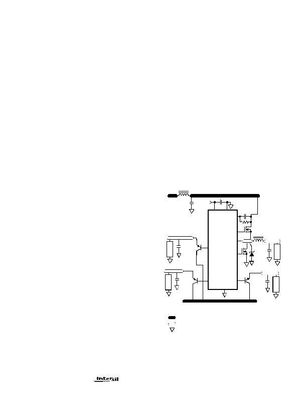
A multi-layer printed circuit board is recommended. Figure 7
shows the connections of the critical components in the
converter. Note that the capacitors C
IN
and C
OUT
each can
represent numerous physical capacitors. Dedicate one
solid layer for a ground plane and make all critical
component ground connections with vias to this layer.
Dedicate another solid layer as a power plane and break
this plane into smaller islands of common voltage levels.
The power plane should support the input power and
output power nodes. Use copper filled polygons on the top
and bottom circuit layers for the PHASE nodes, but do not
unnecessarily oversize these particular islands. Since the
PHASE nodes are subjected to very high dv/dt voltages,
the stray capacitor formed between these islands and the
surrounding circuitry will tend to couple switching noise.
Use the remaining printed circuit layers for small signal
wiring. The wiring traces from the control IC to the
MOSFET gate and source should be sized to carry 2A peak
currents.
2k&
R
S
R
P
?/DIV>
R
S
R
P
+
---------------------- 5k&
<
<
FIGURE 7. PRINTED CIRCUIT BOARD POWER PLANES AND
ISLANDS
V
OUT1
Q1
Q2
Q3
Q4
+12V
C
VCC
VIA CONNECTION TO GROUND PLANE
ISLAND ON POWER PLANE LAYER
ISLAND ON CIRCUIT OR POWER PLANE LAYER
L
OUT
C
OUT1
CR1
ISL6521
C
IN
C
OUT2
V
OUT2
V
OUT3
+5V
IN
PGND
LGATE
UGATE
PHASE
DRIVE3
KEY
GND
VCC
DRIVE2
OCSET
R
OCSET
C
OCSET
V
OUT4
DRIVE4
+3.3V
IN
L
IN
Q5
C
OUT3
C
OUT4
+
+
+
+
+
ISL6521
相关PDF资料 |
PDF描述 |
|---|---|
| HIP6021CBZ-T | IC REG QD BCK/LINEAR 28-SOIC |
| HIP6521CBZ-T | IC REG QD BCK/LINEAR SYNC 16SOIC |
| ACM31DTMT | CONN EDGECARD 62POS R/A .156 SLD |
| RSA36DRMT-S273 | CONN EDGECARD 72POS .125 SQ WW |
| RMA36DRMT-S273 | CONN EDGECARD 72POS .125 SQ WW |
相关代理商/技术参数 |
参数描述 |
|---|---|
| ISL6522ACB | 功能描述:IC REG CTRLR BST PWM VM 14-SOIC RoHS:否 类别:集成电路 (IC) >> PMIC - 稳压器 - DC DC 切换控制器 系列:- 标准包装:4,000 系列:- PWM 型:电压模式 输出数:1 频率 - 最大:1.5MHz 占空比:66.7% 电源电压:4.75 V ~ 5.25 V 降压:是 升压:无 回扫:无 反相:无 倍增器:无 除法器:无 Cuk:无 隔离:无 工作温度:-40°C ~ 85°C 封装/外壳:40-VFQFN 裸露焊盘 包装:带卷 (TR) |
| ISL6522ACB-T | 功能描述:IC REG CTRLR BST PWM VM 14-SOIC RoHS:否 类别:集成电路 (IC) >> PMIC - 稳压器 - DC DC 切换控制器 系列:- 标准包装:4,000 系列:- PWM 型:电压模式 输出数:1 频率 - 最大:1.5MHz 占空比:66.7% 电源电压:4.75 V ~ 5.25 V 降压:是 升压:无 回扫:无 反相:无 倍增器:无 除法器:无 Cuk:无 隔离:无 工作温度:-40°C ~ 85°C 封装/外壳:40-VFQFN 裸露焊盘 包装:带卷 (TR) |
| ISL6522ACR | 功能描述:IC REG CTRLR BST PWM VM 16-QFN RoHS:否 类别:集成电路 (IC) >> PMIC - 稳压器 - DC DC 切换控制器 系列:- 标准包装:4,000 系列:- PWM 型:电压模式 输出数:1 频率 - 最大:1.5MHz 占空比:66.7% 电源电压:4.75 V ~ 5.25 V 降压:是 升压:无 回扫:无 反相:无 倍增器:无 除法器:无 Cuk:无 隔离:无 工作温度:-40°C ~ 85°C 封装/外壳:40-VFQFN 裸露焊盘 包装:带卷 (TR) |
| ISL6522ACR-T | 功能描述:IC REG CTRLR BST PWM VM 16-QFN RoHS:否 类别:集成电路 (IC) >> PMIC - 稳压器 - DC DC 切换控制器 系列:- 标准包装:4,000 系列:- PWM 型:电压模式 输出数:1 频率 - 最大:1.5MHz 占空比:66.7% 电源电压:4.75 V ~ 5.25 V 降压:是 升压:无 回扫:无 反相:无 倍增器:无 除法器:无 Cuk:无 隔离:无 工作温度:-40°C ~ 85°C 封装/外壳:40-VFQFN 裸露焊盘 包装:带卷 (TR) |
| ISL6522BCB | 功能描述:IC REG CTRLR BST PWM VM 14-SOIC RoHS:否 类别:集成电路 (IC) >> PMIC - 稳压器 - DC DC 切换控制器 系列:- 标准包装:4,000 系列:- PWM 型:电压模式 输出数:1 频率 - 最大:1.5MHz 占空比:66.7% 电源电压:4.75 V ~ 5.25 V 降压:是 升压:无 回扫:无 反相:无 倍增器:无 除法器:无 Cuk:无 隔离:无 工作温度:-40°C ~ 85°C 封装/外壳:40-VFQFN 裸露焊盘 包装:带卷 (TR) |
发布紧急采购,3分钟左右您将得到回复。