- 您现在的位置:买卖IC网 > PDF目录15068 > ISL6522ACB-T (Intersil)IC REG CTRLR BST PWM VM 14-SOIC PDF资料下载
参数资料
| 型号: | ISL6522ACB-T |
| 厂商: | Intersil |
| 文件页数: | 10/13页 |
| 文件大小: | 0K |
| 描述: | IC REG CTRLR BST PWM VM 14-SOIC |
| 标准包装: | 2,500 |
| PWM 型: | 电压模式 |
| 输出数: | 1 |
| 频率 - 最大: | 1MHz |
| 占空比: | 100% |
| 电源电压: | 10.8 V ~ 13.2 V |
| 降压: | 是 |
| 升压: | 是 |
| 回扫: | 无 |
| 反相: | 无 |
| 倍增器: | 无 |
| 除法器: | 无 |
| Cuk: | 无 |
| 隔离: | 无 |
| 工作温度: | 25°C ~ 70°C |
| 封装/外壳: | 14-SOIC(0.154",3.90mm 宽) |
| 包装: | 带卷 (TR) |
�� �
�
�ISL6522A�
�should� be� at� least� 1.25� times� greater� than� the� maximum�
�input� voltage� and� a� voltage� rating� of� 1.5� times� is� a�
�conservative� guideline.� The� RMS� current� rating� requirement�
�for� the� input� capacitor� of� a� buck� regulator� is� approximately�
�1/2� the� DC� load� current.�
�For� a� through-hole� design,� several� electrolytic� capacitors�
�(Panasonic� HFQ� series� or� Nichicon� PL� series� or� Sanyo� MV-GX�
�or� equivalent)� may� be� needed.� For� surface� mount� designs,�
�solid� tantalum� capacitors� can� be� used,� but� caution� must� be�
�exercised� with� regard� to� the� capacitor� surge� current� rating.�
�These� capacitors� must� be� capable� of� handling� the� surge-�
�current� at� power-up.� The� TPS� series� available� from� AVX,� and�
�the� 593D� series� from� Sprague� are� both� surge� current� tested.�
�MOSFET� Selection/Considerations�
�The� ISL6522A� requires� two� N-Channel� power� MOSFETs.�
�These� should� be� selected� based� upon� r� DS(ON)� ,� gate� supply�
�requirements,� and� thermal� management� requirements.�
�Standard-gate� MOSFETs� are� normally� recommended� for�
�use� with� the� ISL6522A.� However,� logic-level� gate� MOSFETs�
�can� be� used� under� special� circumstances.� The� input� voltage,�
�upper� gate� drive� level,� and� the� MOSFETs� absolute� gate-to-�
�source� voltage� rating� determine� whether� logic-level�
�MOSFETs� are� appropriate.�
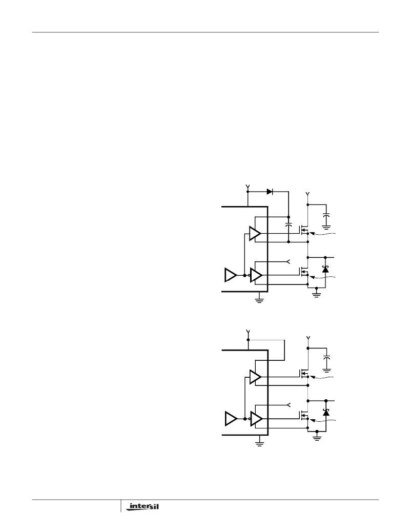
�Figure� 9� shows� the� upper� gate� drive� (BOOT� pin)� supplied� by�
�a� bootstrap� circuit� from� V� CC� .� The� boot� capacitor,� C� BOOT�
�develops� a� floating� supply� voltage� referenced� to� the� PHASE�
�pin.� This� supply� is� refreshed� each� cycle� to� a� voltage� of� V� CC�
�less� the� boot� diode� drop� (V� D� )� when� the� lower� MOSFET,� Q2�
�turns� on.� A� logic-level� MOSFET� can� only� be� used� for� Q1� if�
�the� MOSFETs� absolute� gate-to-source� voltage� rating�
�exceeds� the� maximum� voltage� applied� to� V� CC� .� For� Q2,� a�
�logic-level� MOSFET� can� be� used� if� its� absolute� gate-to-�
�source� voltage� rating� exceeds� the� maximum� voltage� applied�
�to� PVCC.�
�+12V� D� BOOT�
�In� high-current� applications,� the� MOSFET� power� dissipation,�
�package� selection� and� heatsink� are� the� dominant� design�
�VCC�
�+�
�V� D�
�-�
�+5V� OR� +12V�
�factors.� The� power� dissipation� includes� two� loss�
�components;� conduction� loss� and� switching� loss.� The�
�conduction� losses� are� the� largest� component� of� power�
�dissipation� for� both� the� upper� and� the� lower� MOSFETs.�
�These� losses� are� distributed� between� the� two� MOSFETs�
�ISL6522A�
�BOOT�
�UGATE�
�PHASE�
�C� BOOT�
�Q1�
�NOTE:�
�V� G-S� ≈� V� CC� -� V� D�
�according� to� duty� factor.� The� switching� losses� seen� when�
�sourcing� current� will� be� different� from� the� switching� losses� seen�
�+5V�
�PVCC� OR� +12V�
�when� sinking� current.� When� sourcing� current,� the� upper�
�MOSFET� realizes� most� of� the� switching� losses.� The� lower�
�switch� realizes� most� of� the� switching� losses� when� the� converter�
�-�
�+�
�LGATE�
�PGND�
�Q2�
�D2�
�NOTE:�
�V� G-S� ≈� PVCC�
�is� sinking� current� (see� the� equations� below).�
�P� UPPER� =� Io� � r� DS� (� ON� )� � D� +� ---� ?� Io� � V� IN� � t� SW� � F� S�
�Losses� while� Sourcing� Current�
�2� 1�
�2�
�GND�
�FIGURE� 9.� UPPER� GATE� DRIVE� -� BOOTSTRAP� OPTION�
�P� LOWER� =� Io� 2� x� r� DS(ON)� x� (1� -� D)�
�+12V�
�Losses� while� Sinking� Current�
�P� UPPER� =� Io� 2� x� r� DS(ON)� x� D�
�VCC�
�+5V� OR� LESS�
�P� LOWER� =� Io� ×� r� DS� (� ON� )� ×� (� 1� –� D� )� +� ---� ?� Io� ×� V� IN� ×� t� SW� ×� F� S�
�2� 1�
�2�
�Where:� D� is� the� duty� cycle� =� V� OUT� /� V� IN� ,�
�t� SW� is� the� switching� interval,� and�
�F� S� is� the� switching� frequency.�
�These� equations� assume� linear� voltage-current� transitions� and�
�do� not� adequately� model� power� loss� due� the� reverse-recovery�
�ISL6522A�
�BOOT�
�UGATE�
�PHASE�
�+5V�
�OR� +12V�
�PVCC�
�Q1�
�NOTE:�
�V� G-S� ≈� V� CC� -� 5V�
�of� the� upper� and� lower� MOSFET’s� body� diode.� The�
�gate-charge� losses� are� dissipated� by� the� ISL6522A� and� do� not�
�heat� the� MOSFETs.� However,� large� gate-charge� increases� the�
�-�
�+�
�LGATE�
�PGND�
�Q2�
�D2�
�NOTE:�
�V� G-S� ≈� PVCC�
�switching� interval,� t� SW� which� increases� the� upper� MOSFET�
�switching� losses.� Ensure� that� both� MOSFETs� are� within� their�
�maximum� junction� temperature� at� high� ambient� temperature� by�
�calculating� the� temperature� rise� according� to� package� thermal-�
�resistance� specifications.� A� separate� heatsink� may� be�
�necessary� depending� upon� MOSFET� power,� package� type,�
�ambient� temperature� and� air� flow.�
�10�
�GND�
�FIGURE� 10.� UPPER� GATE� DRIVE� -� DIRECT� V� CC� DRIVE� OPTION�
�Figure� 10� shows� the� upper� gate� drive� supplied� by� a� direct�
�connection� to� V� CC� .� This� option� should� only� be� used� in�
�converter� systems� where� the� main� input� voltage� is� +5V� DC� or�
�less.� The� peak� upper� gate-to-source� voltage� is� approximately�
�FN9122.2�
�April� 13,� 2005�
�相关PDF资料 |
PDF描述 |
|---|---|
| ISL6522ACB | IC REG CTRLR BST PWM VM 14-SOIC |
| VI-J4T-EY-F4 | CONVERTER MOD DC/DC 6.5V 50W |
| X4043PZ-2.7 | IC SUPERVISOR CPU 4K EE 8-DIP |
| RBM28DRKN-S13 | CONN EDGECARD 56POS .156 EXTEND |
| VI-2VY-EX-B1 | CONVERTER MOD DC/DC 3.3V 49.5W |
相关代理商/技术参数 |
参数描述 |
|---|---|
| ISL6522ACR | 功能描述:IC REG CTRLR BST PWM VM 16-QFN RoHS:否 类别:集成电路 (IC) >> PMIC - 稳压器 - DC DC 切换控制器 系列:- 标准包装:4,000 系列:- PWM 型:电压模式 输出数:1 频率 - 最大:1.5MHz 占空比:66.7% 电源电压:4.75 V ~ 5.25 V 降压:是 升压:无 回扫:无 反相:无 倍增器:无 除法器:无 Cuk:无 隔离:无 工作温度:-40°C ~ 85°C 封装/外壳:40-VFQFN 裸露焊盘 包装:带卷 (TR) |
| ISL6522ACR-T | 功能描述:IC REG CTRLR BST PWM VM 16-QFN RoHS:否 类别:集成电路 (IC) >> PMIC - 稳压器 - DC DC 切换控制器 系列:- 标准包装:4,000 系列:- PWM 型:电压模式 输出数:1 频率 - 最大:1.5MHz 占空比:66.7% 电源电压:4.75 V ~ 5.25 V 降压:是 升压:无 回扫:无 反相:无 倍增器:无 除法器:无 Cuk:无 隔离:无 工作温度:-40°C ~ 85°C 封装/外壳:40-VFQFN 裸露焊盘 包装:带卷 (TR) |
| ISL6522BCB | 功能描述:IC REG CTRLR BST PWM VM 14-SOIC RoHS:否 类别:集成电路 (IC) >> PMIC - 稳压器 - DC DC 切换控制器 系列:- 标准包装:4,000 系列:- PWM 型:电压模式 输出数:1 频率 - 最大:1.5MHz 占空比:66.7% 电源电压:4.75 V ~ 5.25 V 降压:是 升压:无 回扫:无 反相:无 倍增器:无 除法器:无 Cuk:无 隔离:无 工作温度:-40°C ~ 85°C 封装/外壳:40-VFQFN 裸露焊盘 包装:带卷 (TR) |
| ISL6522BCB-T | 功能描述:IC REG CTRLR BST PWM VM 14-SOIC RoHS:否 类别:集成电路 (IC) >> PMIC - 稳压器 - DC DC 切换控制器 系列:- 标准包装:4,000 系列:- PWM 型:电压模式 输出数:1 频率 - 最大:1.5MHz 占空比:66.7% 电源电压:4.75 V ~ 5.25 V 降压:是 升压:无 回扫:无 反相:无 倍增器:无 除法器:无 Cuk:无 隔离:无 工作温度:-40°C ~ 85°C 封装/外壳:40-VFQFN 裸露焊盘 包装:带卷 (TR) |
| ISL6522BCBZ | 功能描述:IC REG CTRLR BST PWM VM 14-SOIC RoHS:是 类别:集成电路 (IC) >> PMIC - 稳压器 - DC DC 切换控制器 系列:- 标准包装:75 系列:- PWM 型:电流模式 输出数:1 频率 - 最大:1MHz 占空比:81% 电源电压:4.3 V ~ 13.5 V 降压:是 升压:是 回扫:是 反相:无 倍增器:无 除法器:无 Cuk:无 隔离:无 工作温度:0°C ~ 70°C 封装/外壳:8-SOIC(0.154",3.90mm 宽) 包装:管件 产品目录页面:1051 (CN2011-ZH PDF) 其它名称:296-2543-5 |
发布紧急采购,3分钟左右您将得到回复。