- 您现在的位置:买卖IC网 > PDF目录15194 > ISL6522BIBZ-T (Intersil)IC REG CTRLR BST PWM VM 14-SOIC PDF资料下载
参数资料
| 型号: | ISL6522BIBZ-T |
| 厂商: | Intersil |
| 文件页数: | 8/15页 |
| 文件大小: | 0K |
| 描述: | IC REG CTRLR BST PWM VM 14-SOIC |
| 标准包装: | 2,500 |
| PWM 型: | 电压模式 |
| 输出数: | 1 |
| 频率 - 最大: | 1MHz |
| 占空比: | 100% |
| 电源电压: | 10.8 V ~ 13.2 V |
| 降压: | 是 |
| 升压: | 是 |
| 回扫: | 无 |
| 反相: | 无 |
| 倍增器: | 无 |
| 除法器: | 无 |
| Cuk: | 无 |
| 隔离: | 无 |
| 工作温度: | -40°C ~ 85°C |
| 封装/外壳: | 14-SOIC(0.154",3.90mm 宽) |
| 包装: | 带卷 (TR) |
�� �
�
�ISL6522B�
�I� PEAK� =� ---------------------------------------------------�
�Overcurrent� Protection�
�The� overcurrent� function� protects� the� converter� from� a�
�shorted� output� by� using� the� upper� MOSFETs� on-resistance,�
�r� DS(ON)� to� monitor� the� current.� This� method� enhances� the�
�converter� ’s� efficiency� and� reduces� cost� by� eliminating� a�
�current� sensing� resistor.�
�The� overcurrent� function� cycles� the� soft-start� function� in� a�
�hiccup� mode� to� provide� fault� protection.� A� resistor� (R� OCSET� )�
�programs� the� overcurrent� trip� level.� An� internal� 200� μ� A�
�(typical)� current� sink� develops� a� voltage� across� R� OCSET� that�
�is� in� reference� to� V� IN� .� When� the� voltage� across� the� upper�
�MOSFET� (also� referenced� to� V� IN� )� exceeds� the� voltage�
�across� R� OCSET� ,� the� overcurrent� function� initiates� a� soft-start�
�sequence.� The� soft-start� function� discharges� C� SS� with� a�
�10� μ� A� current� sink� and� inhibits� PWM� operation.� The� soft-start�
�function� recharges� C� SS� ,� and� PWM� operation� resumes� with�
�the� error� amplifier� clamped� to� the� SS� voltage.� Should� an�
�overload� occur� while� recharging� C� SS� ,� the� soft-start� function�
�inhibits� PWM� operation� while� fully� charging� C� SS� to� 4V� to�
�complete� its� cycle.� Figure� 4� shows� this� operation� with� an�
�overload� condition.� Note� that� the� inductor� current� increases�
�to� over� 15A� during� the� C� SS� charging� interval� and� causes� an�
�overcurrent� trip.� The� converter� dissipates� very� little� power�
�with� this� method.� The� measured� input� power� for� the�
�conditions� of� Figure� 4� is� 2.5W.�
�The� overcurrent� function� will� trip� at� a� peak� inductor� current�
�(I� PEAK)� determined� by:�
�I� OCSET� ?� R� OCSET�
�r� DS� (� ON� )�
�where� I� OCSET� is� the� internal� OCSET� current� source� (200� μ� A�
�is� typical).� The� OC� trip� point� varies� mainly� due� to� the�
�MOSFETs� r� DS(ON)� variations.� To� avoid� overcurrent� tripping�
�in� the� normal� operating� load� range,� find� the� R� OCSET� resistor�
�from� the� equation� above� with:�
�The� maximum� r� DS(ON)� at� the� highest� junction� temperature.�
�1.� The� minimum� I� OCSET� from� the� specification� table.�
�2.� Determine� I� PEAK� for� I� PEAK� >� I� OUT� (� MAX� )� +� (� ?� I� )� ?� 2� ,�
�where� ?� I� is� the� output� inductor� ripple� current.�
�When� the� converter� is� sinking� current,� it� is� behaving� as� a�
�boost� converter� that� is� regulating� its� input� voltage.� This�
�means� that� the� converter� is� boosting� current� into� the� V� IN� rail,�
�the� voltage� that� is� being� down-converted.� If� there� is� nowhere�
�for� this� current� to� go,� such� as� to� other� distributed� loads� on�
�the� V� IN� rail,� through� a� voltage� limiting� protection� device,� or�
�other� methods,� the� capacitance� on� the� V� IN� bus� will� absorb�
�the� current.� This� situation� will� cause� the� voltage� level� of� the�
�V� IN� rail� to� increase.� If� the� voltage� level� of� the� rail� is� boosted�
�to� a� level� that� exceeds� the� maximum� voltage� rating� of� the�
�MOSFETs� or� the� input� capacitors,� damage� may� occur� to�
�these� parts.� If� the� bias� voltage� for� the� ISL6522B� comes� from�
�the� V� IN� rail,� then� the� maximum� voltage� rating� of� the�
�ISL6522B� may� be� exceeded� and� the� IC� will� experience� a�
�catastrophic� failure� and� the� converter� will� no� longer� be�
�operational.� Ensuring� that� there� is� a� path� for� the� current� to�
�follow� other� than� the� capacitance� on� the� rail� will� prevent�
�these� failure� modes.�
�Application� Guidelines�
�Layout� Considerations�
�As� in� any� high� frequency� switching� converter,� layout� is� very�
�important.� Switching� current� from� one� power� device� to�
�another� can� generate� voltage� transients� across� the�
�impedances� of� the� interconnecting� bond� wires� and� circuit�
�traces.� These� interconnecting� impedances� should� be�
�minimized� by� using� wide,� short� printed� circuit� traces.� The�
�critical� components� should� be� located� as� close� together� as�
�possible� using� ground� plane� construction� or� single� point�
�grounding.�
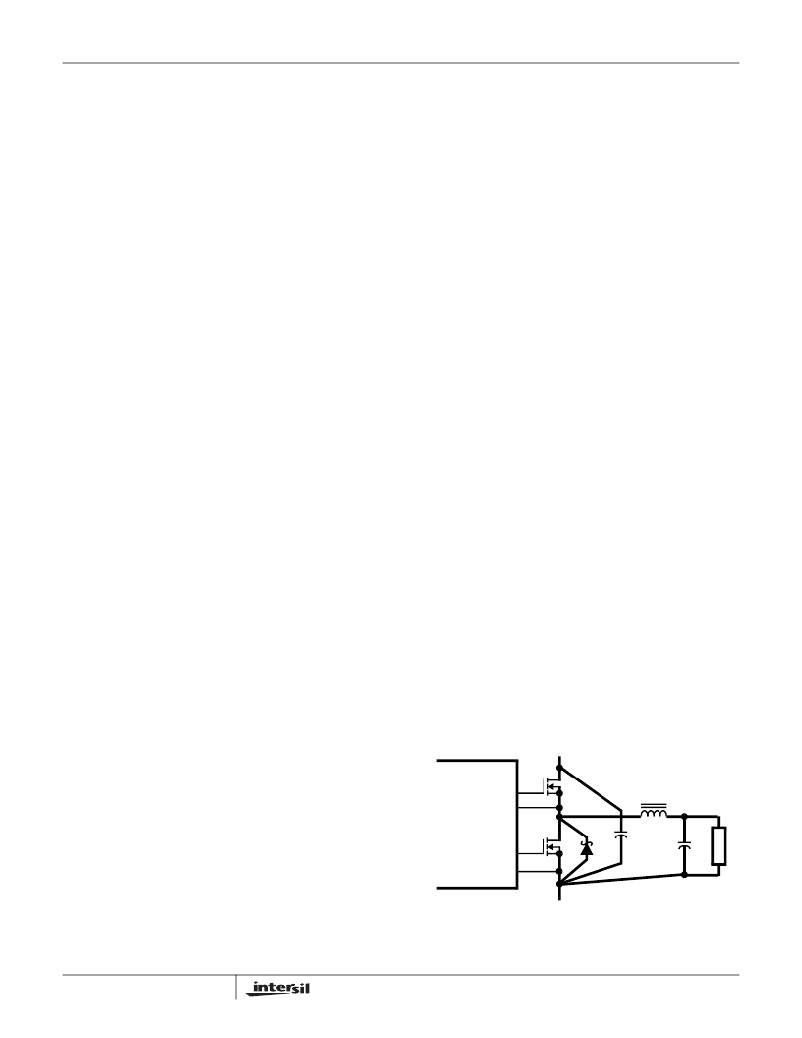
�Figure� 5� shows� the� critical� power� components� of� the�
�converter.� To� minimize� the� voltage� overshoot� the�
�interconnecting� wires� indicated� by� heavy� lines� should� be� part�
�of� ground� or� power� plane� in� a� printed� circuit� board.� The�
�components� shown� in� Figure� 6� should� be� located� as� close�
�together� as� possible.� Please� note� that� the� capacitors� C� IN�
�and� C� O� each� represent� numerous� physical� capacitors.�
�Locate� the� ISL6522B� within� three� inches� of� the� MOSFETs,�
�Q1� and� Q2.� The� circuit� traces� for� the� MOSFETs’� gate� and�
�source� connections� from� the� ISL6522B� must� be� sized� to�
�handle� up� to� 1A� peak� current.�
�For� an� equation� for� the� ripple� current� see� the� section� under�
�component� guidelines� titled� Output� Inductor� Selection� .�
�ISL6522B�
�V� IN�
�A� small� ceramic� capacitor� should� be� placed� in� parallel� with�
�R� OCSET� to� smooth� the� voltage� across� R� OCSET� in� the�
�presence� of� switching� noise� on� the� input� voltage.�
�UGATE�
�PHASE�
�Q1�
�L� O�
�V� OUT�
�Current� Sinking�
�LGATE�
�Q2�
�D2�
�C� IN�
�C� O�
�The� ISL6522B� incorporates� a� MOSFET� shoot-through�
�protection� method� which� allows� a� converter� to� sink� current�
�as� well� as� source� current.� Care� should� be� exercised� when�
�designing� a� converter� with� the� ISL6522B� when� it� is� known�
�that� the� converter� may� sink� current.�
�8�
�PGND�
�RETURN�
�FIGURE� 5.� PRINTED� CIRCUIT� BOARD� POWER� AND�
�GROUND� PLANES� OR� ISLANDS�
�相关PDF资料 |
PDF描述 |
|---|---|
| ISL6522BCRZ-T | IC REG CTRLR BST PWM VM 16-QFN |
| ISL6522BCBZ-T | IC REG CTRLR BST PWM VM 14-SOIC |
| RCC20DRYH-S93 | CONN EDGECARD 40POS DIP .100 SLD |
| ISL88002IE22Z-TK | IC VOLT SUPERVISOR 2.19V SC-70 |
| ISL6520IBZ-T | IC REG CTRLR BUCK PWM VM 8-SOIC |
相关代理商/技术参数 |
参数描述 |
|---|---|
| ISL6522BIBZ-TS2698 | 功能描述:IC REG CTRLR BST PWM VM 14-SOIC RoHS:是 类别:集成电路 (IC) >> PMIC - 稳压器 - DC DC 切换控制器 系列:- 产品培训模块:Lead (SnPb) Finish for COTS Obsolescence Mitigation Program 标准包装:2,500 系列:- PWM 型:电流模式 输出数:1 频率 - 最大:275kHz 占空比:50% 电源电压:18 V ~ 110 V 降压:无 升压:无 回扫:无 反相:无 倍增器:无 除法器:无 Cuk:无 隔离:是 工作温度:-40°C ~ 85°C 封装/外壳:8-SOIC(0.154",3.90mm 宽) 包装:带卷 (TR) |
| ISL6522BIR | 功能描述:IC REG CTRLR BST PWM VM 16-QFN RoHS:否 类别:集成电路 (IC) >> PMIC - 稳压器 - DC DC 切换控制器 系列:- 标准包装:4,000 系列:- PWM 型:电压模式 输出数:1 频率 - 最大:1.5MHz 占空比:66.7% 电源电压:4.75 V ~ 5.25 V 降压:是 升压:无 回扫:无 反相:无 倍增器:无 除法器:无 Cuk:无 隔离:无 工作温度:-40°C ~ 85°C 封装/外壳:40-VFQFN 裸露焊盘 包装:带卷 (TR) |
| ISL6522BIR-T | 功能描述:IC REG CTRLR BST PWM VM 16-QFN RoHS:否 类别:集成电路 (IC) >> PMIC - 稳压器 - DC DC 切换控制器 系列:- 标准包装:4,000 系列:- PWM 型:电压模式 输出数:1 频率 - 最大:1.5MHz 占空比:66.7% 电源电压:4.75 V ~ 5.25 V 降压:是 升压:无 回扫:无 反相:无 倍增器:无 除法器:无 Cuk:无 隔离:无 工作温度:-40°C ~ 85°C 封装/外壳:40-VFQFN 裸露焊盘 包装:带卷 (TR) |
| ISL6522BIRZ | 功能描述:IC REG CTRLR BST PWM VM 16-QFN RoHS:是 类别:集成电路 (IC) >> PMIC - 稳压器 - DC DC 切换控制器 系列:- 产品培训模块:Lead (SnPb) Finish for COTS Obsolescence Mitigation Program 标准包装:2,500 系列:- PWM 型:电流模式 输出数:1 频率 - 最大:275kHz 占空比:50% 电源电压:18 V ~ 110 V 降压:无 升压:无 回扫:无 反相:无 倍增器:无 除法器:无 Cuk:无 隔离:是 工作温度:-40°C ~ 85°C 封装/外壳:8-SOIC(0.154",3.90mm 宽) 包装:带卷 (TR) |
| ISL6522BIRZR5190 | 功能描述:IC REG CTRLR BST PWM VM 16-QFN RoHS:是 类别:集成电路 (IC) >> PMIC - 稳压器 - DC DC 切换控制器 系列:- 产品培训模块:Lead (SnPb) Finish for COTS Obsolescence Mitigation Program 标准包装:2,500 系列:- PWM 型:电流模式 输出数:1 频率 - 最大:275kHz 占空比:50% 电源电压:18 V ~ 110 V 降压:无 升压:无 回扫:无 反相:无 倍增器:无 除法器:无 Cuk:无 隔离:是 工作温度:-40°C ~ 85°C 封装/外壳:8-SOIC(0.154",3.90mm 宽) 包装:带卷 (TR) |
发布紧急采购,3分钟左右您将得到回复。