- 您现在的位置:买卖IC网 > PDF目录15197 > ISL6526AIRZ-TK (Intersil)IC REG CTRLR BUCK PWM VM 16-QFN PDF资料下载
参数资料
| 型号: | ISL6526AIRZ-TK |
| 厂商: | Intersil |
| 文件页数: | 12/15页 |
| 文件大小: | 0K |
| 描述: | IC REG CTRLR BUCK PWM VM 16-QFN |
| 标准包装: | 1,000 |
| PWM 型: | 电压模式 |
| 输出数: | 1 |
| 频率 - 最大: | 650kHz |
| 占空比: | 100% |
| 电源电压: | 2.97 V ~ 3.63 V |
| 降压: | 是 |
| 升压: | 无 |
| 回扫: | 无 |
| 反相: | 无 |
| 倍增器: | 无 |
| 除法器: | 无 |
| Cuk: | 无 |
| 隔离: | 无 |
| 工作温度: | 0°C ~ 70°C |
| 封装/外壳: | 16-VQFN 裸露焊盘 |
| 包装: | 带卷 (TR) |
�� �
�
�ISL6526,� ISL6526A�
�P� LOWER� =� Io� ×� r� DS� (� ON� )� ×� (� 1� –� D� )� +� ---� ?� Io� ×� V� IN� ×� t� SW� ×� f� s�
�--------------� � ?� I� OUT�
�+� ------� � ?� -----------------------------� � --------------� ?� ?�
�I� RMS�
�?�
�V� IN� ?� ?�
�?�
�L� � f� s�
�V� IN�
�input� voltage� and� a� voltage� rating� of� 1.5� times� is� a�
�conservative� guideline.� The� RMS� current� rating� requirement�
�for� the� input� capacitor� of� a� buck� regulator� is� approximately�
�1/2� the� DC� load� current.�
�The� maximum� RMS� current� required� by� the� regulator� may� be�
�closely� approximated� using� Equation� 15:�
�V� OUT� 2� 1� V� IN� –� V� OUT� V� OUT� 2�
�=�
�MAX� MAX� 12�
�(EQ.� 15)�
�For� a� through� hole� design,� several� electrolytic� capacitors� may�
�be� needed.� For� surface� mount� designs,� solid� tantalum�
�capacitors� can� be� used,� but� caution� must� be� exercised� with�
�regard� to� the� capacitor� surge� current� rating.� These� capacitors�
�must� be� capable� of� handling� the� surge-current� at� power-up.�
�Some� capacitor� series� available� from� reputable� manufacturers�
�are� surge� current� tested.�
�MOSFET� Selection/Considerations�
�The� ISL6526,� ISL6526A� require� two� N-Channel� power�
�MOSFETs.� These� should� be� selected� based� upon� r� DS(ON)� ,�
�gate� supply� requirements,� and� thermal� management�
�requirements.�
�In� high-current� applications,� the� MOSFET� power� dissipation,�
�package� selection� and� heatsink� are� the� dominant� design�
�factors.� The� power� dissipation� includes� two� loss� components;�
�conduction� loss� and� switching� loss.� The� conduction� losses� are�
�Losses while Sinking Current�
�P� UPPER� =� Io� 2� x� r� DS(ON)� x� D�
�2� 1�
�2�
�Where:� D� is� the� duty� cycle� =� V� OUT� /V� IN� ,�
�t� SW� is� the� combined� switch� ON� and� OFF� time,� and�
�f� s� is� the� switching� frequency.�
�(EQ.� 17)�
�Given� the� reduced� available� gate� bias� voltage� (5V),� logic-level�
�or� sub-logic-level� transistors� should� be� used� for� both�
�N-MOSFETs.� Caution� should� be� exercised� with� devices�
�exhibiting� very� low� V� GS(ON)� characteristics.� The� shoot-through�
�protection� present� aboard� the� ISL6526,� ISL6526A� may� be�
�circumvented� by� these� MOSFETs� if� they� have� large� parasitic�
�impedances� and/or� capacitances� that� would� inhibit� the� gate� of�
�the� MOSFET� from� being� discharged� below� its� threshold� level�
�before� the� complementary� MOSFET� is� turned� on.�
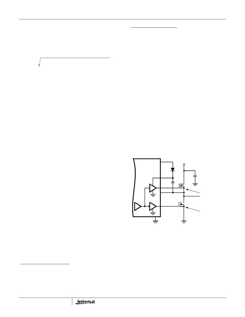
�Bootstrap� Component� Selection�
�External� bootstrap� components,� a� diode� and� capacitor,� are�
�required� to� provide� sufficient� gate� enhancement� to� the� upper�
�MOSFET.� The� internal� MOSFET� gate� driver� is� supplied� by� the�
�external� bootstrap� circuitry,� as� shown� in� Figure� 7.� The� boot�
�capacitor,� C� BOOT� ,� develops� a� floating� supply� voltage�
�referenced� to� the� PHASE� pin.� This� supply� is� refreshed� each�
�cycle,� when� D� BOOT� conducts,� to� a� voltage� of� CPVOUT� less� the�
�boot� diode� drop,� V� D� ,� plus� the� voltage� rise� across� Q� LOWER� .�
�the� largest� component� of� power� dissipation� for� both� the� upper�
�and� the� lower� MOSFETs.� These� losses� are� distributed�
�between� the� two� MOSFETs� according� to� duty� factor.� The�
�ISL6526,�
�ISL6526A�
�CPVOUT�
�D� BOOT�
�+�
�V� D�
�V� IN�
�switching� losses� seen� when� sourcing� current� will� be� different�
�from� the� switching� losses� seen� when� sinking� current.� When�
�sourcing� current,� the� upper� MOSFET� realizes� most� of� the�
�switching� losses.� The� lower� switch� realizes� most� of� the�
�switching� losses� when� the� converter� is� sinking� current� (see�
�Equations� 16� and� 17).� These� equations� assume� linear�
�voltage-current� transitions� and� do� not� adequately� model�
�power� loss� due� the� reverse-recovery� of� the� upper� and� lower�
�MOSFET’s� body� diode.� The� gate-charge� losses� are�
�dissipated� by� the� ISL6526,� ISL6526A� and� don't� heat� the�
�MOSFETs.� However,� large� gate-charge� increases� the�
�-�
�+�
�BOOT�
�UGATE�
�PHASE�
�LGATE�
�GND�
�-�
�C� BOOT�
�Q� UPPER�
�Q� LOWER�
�NOTE:�
�V� G-S� =� V� CC� -V� D�
�NOTE:�
�V� G-S� =� V� CC�
�P� UPPER� =� Io� � r� DS� (� ON� )� � D� +� ---� ?� Io� � V� IN� � t� SW� � f� s�
�switching� interval,� t� SW� which� increases� the� MOSFET�
�switching� losses.� Ensure� that� both� MOSFETs� are� within� their�
�maximum� junction� temperature� at� high� ambient� temperature�
�by� calculating� the� temperature� rise� according� to� package�
�thermal-resistance� specifications.� A� separate� heatsink� may� be�
�necessary� depending� upon� MOSFET� power,� package� type,�
�ambient� temperature� and� air� flow.�
�Losses while Sourcing Current�
�2� 1�
�2�
�FIGURE� 7.� UPPER� GATE� DRIVE� BOOTSTRAP�
�Just� after� the� PWM� switching� cycle� begins� and� the� charge�
�transfer� from� the� bootstrap� capacitor� to� the� gate� capacitance�
�is� complete,� the� voltage� on� the� bootstrap� capacitor� is� at� its�
�lowest� point� during� the� switching� cycle.� The� charge� lost� on�
�the� bootstrap� capacitor� will� be� equal� to� the� charge�
�transferred� to� the� equivalent� gate-source� capacitance� of� the�
�upper� MOSFET� as� shown� in� Equation� 18:�
�P� LOWER� =� Io� 2� x� r� DS(ON)� x� (1� -� D)�
�12�
�(EQ.� 16)�
�Q� GATE� =� C� BOOT� ×� (� V� BOOT1� –� V� BOOT2� )�
�(EQ.� 18)�
�FN9055.10�
�November� 24,� 2008�
�相关PDF资料 |
PDF描述 |
|---|---|
| GEC44DRES-S93 | CONN EDGECARD 88POS .100 EYELET |
| ISL6526AIRZ-T | IC REG CTRLR BUCK PWM VM 16-QFN |
| ISL6420IRZ-TK | IC REG CTRLR BUCK PWM VM 20-QFN |
| ISL6420IRZ-T | IC REG CTRLR BUCK PWM VM 20-QFN |
| EBC30DRYI-S93 | CONN EDGECARD 60POS DIP .100 SLD |
相关代理商/技术参数 |
参数描述 |
|---|---|
| ISL6526CB | 功能描述:IC REG CTRLR BUCK PWM VM 14-SOIC RoHS:否 类别:集成电路 (IC) >> PMIC - 稳压器 - DC DC 切换控制器 系列:- 标准包装:4,000 系列:- PWM 型:电压模式 输出数:1 频率 - 最大:1.5MHz 占空比:66.7% 电源电压:4.75 V ~ 5.25 V 降压:是 升压:无 回扫:无 反相:无 倍增器:无 除法器:无 Cuk:无 隔离:无 工作温度:-40°C ~ 85°C 封装/外壳:40-VFQFN 裸露焊盘 包装:带卷 (TR) |
| ISL6526CB-T | 功能描述:电压模式 PWM 控制器 Single Synch Buck RoHS:否 制造商:Texas Instruments 输出端数量:1 拓扑结构:Buck 输出电压:34 V 输出电流: 开关频率: 工作电源电压:4.5 V to 5.5 V 电源电流:600 uA 最大工作温度:+ 125 C 最小工作温度:- 40 C 封装 / 箱体:WSON-8 封装:Reel |
| ISL6526CBZ | 功能描述:电压模式 PWM 控制器 300 KHZ SINGLE PWM W/CHRG PUMP 14LD N RoHS:否 制造商:Texas Instruments 输出端数量:1 拓扑结构:Buck 输出电压:34 V 输出电流: 开关频率: 工作电源电压:4.5 V to 5.5 V 电源电流:600 uA 最大工作温度:+ 125 C 最小工作温度:- 40 C 封装 / 箱体:WSON-8 封装:Reel |
| ISL6526CBZ-T | 功能描述:电压模式 PWM 控制器 300 KHZ SINGLE PWM W/CHRG PUMP 14LD N RoHS:否 制造商:Texas Instruments 输出端数量:1 拓扑结构:Buck 输出电压:34 V 输出电流: 开关频率: 工作电源电压:4.5 V to 5.5 V 电源电流:600 uA 最大工作温度:+ 125 C 最小工作温度:- 40 C 封装 / 箱体:WSON-8 封装:Reel |
| ISL6526CR | 功能描述:IC REG CTRLR BUCK PWM VM 16-QFN RoHS:否 类别:集成电路 (IC) >> PMIC - 稳压器 - DC DC 切换控制器 系列:- 标准包装:4,000 系列:- PWM 型:电压模式 输出数:1 频率 - 最大:1.5MHz 占空比:66.7% 电源电压:4.75 V ~ 5.25 V 降压:是 升压:无 回扫:无 反相:无 倍增器:无 除法器:无 Cuk:无 隔离:无 工作温度:-40°C ~ 85°C 封装/外壳:40-VFQFN 裸露焊盘 包装:带卷 (TR) |
发布紧急采购,3分钟左右您将得到回复。