- 您现在的位置:买卖IC网 > PDF目录22323 > ISL6528CBZS2698 (Intersil)IC REG DL BCK/LINEAR SYNC 8-SOIC PDF资料下载
参数资料
| 型号: | ISL6528CBZS2698 |
| 厂商: | Intersil |
| 文件页数: | 11/13页 |
| 文件大小: | 361K |
| 描述: | IC REG DL BCK/LINEAR SYNC 8-SOIC |
| 标准包装: | 980 |
| 拓扑: | 降压(降压)同步(1),线性(LDO)(1) |
| 功能: | 任何功能 |
| 输出数: | 2 |
| 频率 - 开关: | 600kHz |
| 电压/电流 - 输出 1: | 控制器 |
| 电压/电流 - 输出 2: | 控制器 |
| 带 LED 驱动器: | 无 |
| 带监控器: | 无 |
| 带序列发生器: | 无 |
| 电源电压: | 4.5 V ~ 5.5 V |
| 工作温度: | 0°C ~ 70°C |
| 安装类型: | * |
| 封装/外壳: | 8-SOIC(0.154",3.90mm 宽) |
| 供应商设备封装: | * |
| 包装: | 管件 |
11
FN9038.4
March 9, 2006
load current when the base is fed with the minimum driver
output current.
The main criteria for selection of the linear regulator pass
transistor is package selection for efficient removal of heat.
Select a package and heatsink that maintains the junction
temperature below the rating with a maximum expected
ambient temperature.
The power dissipated in a linear regulator is:
where I
O
is the maximum output current and V
OUT
is the
nominal output voltage of the linear regulator.
Diode Selection (D1)
Rectifier D1 conducts when MOSFET Q1 is off. The diode
should be a Schottky type for low power losses. The power
dissipation in the Schottky rectifier is approximated by:
where I
O
is the maximum output current of the PWM
converter, V
f
is the Schottky forward voltage drop, and D is
the duty cycle of the converter (defined as V
O
/V
IN
).
In addition to power dissipation, package selection and
heatsink requirements are the main design trade-offs in
choosing a Schottky rectifier. Since the three factors are
interrelated, the selection process is an iterative procedure.
The maximum junction temperature of the rectifier must
remain below the manufacturers specified value, typically
125癈. By using the package thermal resistance
specification and the Schottky power dissipation equation,
the junction temperature of the rectifier can be estimated. Be
sure to use the available airflow and ambient temperature to
determine the junction temperature rise.
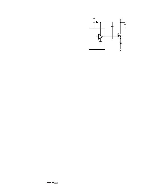
Bootstrap Component Selection
External bootstrap components, a diode and capacitor, are
required to provide sufficient gate enhancement to the
MOSFET. The internal MOSFET gate driver is supplied by
the external bootstrap circuitry as shown in Figure 8. The
boot capacitor, C
BOOT
, develops a floating supply voltage
referenced to the PHASE pin. This supply is refreshed each
cycle, when D1 conducts, to a voltage of VCC less the boot
diode drop, V
D2
, plus the voltage rise across D1.
Just after the PWM switching cycle begins and the charge
transfer from the bootstrap capacitor to the gate capacitance
is complete, the voltage on the bootstrap capacitor is at its
lowest point during the switching cycle. The charge lost on
the bootstrap capacitor will be equal to the charge
transferred to the equivalent gate-source capacitance of the
MOSFET as shown in Equation 19.
where Q
GATE
is the maximum total gate charge of the
MOSFET, C
BOOT
is the bootstrap capacitance, V
BOOT1
is
the bootstrap voltage immediately before turn-on, and
V
BOOT2
is the bootstrap voltage immediately after turn-on.
The bootstrap capacitor begins its refresh cycle when the
gate drive begins to turn off the MOSFET. A refresh cycle
ends when the MOSFET is turned on again, which varies
depending on the switching frequency and duty cycle.
The minimum bootstrap capacitance can be calculated by
rearranging Equation 19 and solving for C
BOOT
.
Typical gate charge values for MOSFETs considered in
these types of applications range from 20100nC. Since the
voltage drop across D2 is offset by the voltage drop across
D1, V
BOOT1
is simply VCC (+5V). A good rule is to keep the
voltage drop across the bootstrap capacitor no greater than
1V during the on-time of the MOSFET. Initial calculations
with V
BOOT2
no less than 4V will quickly help narrow the
bootstrap capacitor range.
For example, consider a MOSFET is chosen with a
maximum gate charge, Q
g
, of 100nC. Limiting the voltage
drop across the bootstrap capacitor to 1V results in a value
of no less than 0.1礔. The tolerance of the ceramic capacitor
should also be considered when selecting the final bootstrap
capacitance value.
A fast recovery diode is recommended when selecting a
bootstrap diode to reduce the impact of reverse recovery
charge loss. Otherwise, the recovery charge, Q
RR
, would
have to be added to the gate charge of the MOSFET and
taken into consideration when calculating the minimum
bootstrap capacitance. Employing a Schottky diode over a
standard diode will also increase the gate drive voltage
available to enhance the MOSFET.
P
LINEAR
I
O
V
IN
V
OUT
(
)
?/DIV>
E
(EQ. 17)
P
CONDUCTION
I
O
V
f
?nbsp 1 D
( )
?/DIV>
E
(EQ. 18)
Q
GATE
C
BOOT
V
BOOT1
V
BOOT2
(
)
?/DIV>
=
(EQ. 19)
Q1
D1
C
BOOT
BOOT
UGATE
PHASE
VCC
+3.3V
+5V
D2
ISL6528
FIGURE 8. UPPER GATE DRIVE
C
BOOT
Q
GATE
V
BOOT1
V
BOOT2
-----------------------------------------------------
e
(EQ. 20)
ISL6528
相关PDF资料 |
PDF描述 |
|---|---|
| V110C8H75BF2 | CONVERTER MOD DC/DC 8V 75W |
| ISL6549IRZ | IC REG DL BCK/LINEAR SYNC 16-QFN |
| ISL6534CRZ | IC REG TRPL BCK/LINEAR 32QFN |
| V110C8H75BF | CONVERTER MOD DC/DC 8V 75W |
| V110C8H75BL3 | CONVERTER MOD DC/DC 8V 75W |
相关代理商/技术参数 |
参数描述 |
|---|---|
| ISL6528CBZ-T | 功能描述:IC REG DL BCK/LINEAR SYNC 8-SOIC RoHS:是 类别:集成电路 (IC) >> PMIC - 稳压器 - 线性 + 切换式 系列:- 标准包装:2,500 系列:- 拓扑:降压(降压)同步(3),线性(LDO)(2) 功能:任何功能 输出数:5 频率 - 开关:300kHz 电压/电流 - 输出 1:控制器 电压/电流 - 输出 2:控制器 电压/电流 - 输出 3:控制器 带 LED 驱动器:无 带监控器:无 带序列发生器:是 电源电压:5.6 V ~ 24 V 工作温度:-40°C ~ 85°C 安装类型:* 封装/外壳:* 供应商设备封装:* 包装:* |
| ISL6528CBZ-TS2698 | 功能描述:IC REG DL BCK/LINEAR SYNC 8-SOIC RoHS:是 类别:集成电路 (IC) >> PMIC - 稳压器 - 线性 + 切换式 系列:- 标准包装:2,500 系列:- 拓扑:降压(降压)同步(3),线性(LDO)(2) 功能:任何功能 输出数:5 频率 - 开关:300kHz 电压/电流 - 输出 1:控制器 电压/电流 - 输出 2:控制器 电压/电流 - 输出 3:控制器 带 LED 驱动器:无 带监控器:无 带序列发生器:是 电源电压:5.6 V ~ 24 V 工作温度:-40°C ~ 85°C 安装类型:* 封装/外壳:* 供应商设备封装:* 包装:* |
| ISL6529ACB | 功能描述:IC REG DL BCK/LINEAR 14-SOIC RoHS:否 类别:集成电路 (IC) >> PMIC - 稳压器 - 线性 + 切换式 系列:- 标准包装:2,500 系列:- 拓扑:降压(降压)同步(3),线性(LDO)(2) 功能:任何功能 输出数:5 频率 - 开关:300kHz 电压/电流 - 输出 1:控制器 电压/电流 - 输出 2:控制器 电压/电流 - 输出 3:控制器 带 LED 驱动器:无 带监控器:无 带序列发生器:是 电源电压:5.6 V ~ 24 V 工作温度:-40°C ~ 85°C 安装类型:* 封装/外壳:* 供应商设备封装:* 包装:* |
| ISL6529ACB-T | 功能描述:IC REG DL BCK/LINEAR 14-SOIC RoHS:否 类别:集成电路 (IC) >> PMIC - 稳压器 - 线性 + 切换式 系列:- 标准包装:2,500 系列:- 拓扑:降压(降压)同步(3),线性(LDO)(2) 功能:任何功能 输出数:5 频率 - 开关:300kHz 电压/电流 - 输出 1:控制器 电压/电流 - 输出 2:控制器 电压/电流 - 输出 3:控制器 带 LED 驱动器:无 带监控器:无 带序列发生器:是 电源电压:5.6 V ~ 24 V 工作温度:-40°C ~ 85°C 安装类型:* 封装/外壳:* 供应商设备封装:* 包装:* |
| ISL6529ACR | 功能描述:IC REG DL BCK/LINEAR SYNC 16-QFN RoHS:否 类别:集成电路 (IC) >> PMIC - 稳压器 - 线性 + 切换式 系列:- 标准包装:2,500 系列:- 拓扑:降压(降压)同步(3),线性(LDO)(2) 功能:任何功能 输出数:5 频率 - 开关:300kHz 电压/电流 - 输出 1:控制器 电压/电流 - 输出 2:控制器 电压/电流 - 输出 3:控制器 带 LED 驱动器:无 带监控器:无 带序列发生器:是 电源电压:5.6 V ~ 24 V 工作温度:-40°C ~ 85°C 安装类型:* 封装/外壳:* 供应商设备封装:* 包装:* |
发布紧急采购,3分钟左右您将得到回复。