参数资料
| 型号: | ISL6530CBZ |
| 厂商: | Intersil |
| 文件页数: | 14/17页 |
| 文件大小: | 0K |
| 描述: | IC CONTROLLER INTEL 24SOIC |
| 标准包装: | 600 |
| 应用: | 控制器,Intel Pentium? III,IV |
| 输入电压: | 4.5 V ~ 5.5 V |
| 输出数: | 2 |
| 输出电压: | 2.5V |
| 工作温度: | 0°C ~ 70°C |
| 安装类型: | 表面贴装 |
| 封装/外壳: | 24-SOIC(0.295",7.50mm 宽) |
| 供应商设备封装: | 24-SOIC |
| 包装: | 管件 |
�� �
�
�ISL6530�
�C� BOOT� ≥� -----------------------------------------------------�
�Ensure� that� both� MOSFETs� are� within� their� maximum� junction�
�temperature� at� high� ambient� temperature� by� calculating� the�
�temperature� rise� according� to� package� thermal-resistance�
�specifications.� A� separate� heatsink� may� be� necessary�
�depending� upon� MOSFET� power,� package� type,� ambient�
�temperature� and� air� flow.�
�Given� the� reduced� available� gate� bias� voltage� (5V),� logic-�
�level� or� sub-logic-level� transistors� should� be� used� for� both� N-�
�MOSFETs.� Caution� should� be� exercised� when� using� devices�
�with� very� low� gate� thresholds� (V� TH� ).� The� shoot-through�
�protection� circuitry� may� be� circumvented� by� these�
�MOSFETs.� Very� high� dv/dt� transitions� on� the� phase� node�
�may� cause� the� Miller� capacitance� to� couple� the� lower� gate�
�with� the� phase� node� and� cause� an� undesireable� turn� on� of�
�the� lower� MOSFET� while� the� upper� MOSFET� is� on.�
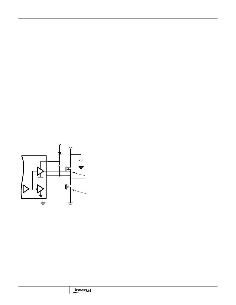
�Bootstrap� Component� Selection�
�External� bootstrap� components,� a� diode� and� capacitor,� are�
�required� to� provide� sufficient� gate� enhancement� to� the� upper�
�MOSFET.� The� internal� MOSFET� gate� driver� is� supplied� by�
�the� external� bootstrap� circuitry� as� shown� in� Figure� 10.� The�
�boot� capacitor,� C� BOOT� ,� develops� a� floating� supply� voltage�
�referenced� to� the� PHASE� pin.� This� supply� is� refreshed� each�
�cycle,� when� D� BOOT� conducts,� to� a� voltage� of� VCC� less� the�
�boot� diode� drop,� V� D� ,� plus� the� voltage� rise� across� Q� LOWER� .�
�The� bootstrap� capacitor� begins� its� refresh� cycle� when� the�
�gate� drive� begins� to� turn-off� the� upper� MOSFET.� A� refresh�
�cycle� ends� when� the� upper� MOSFET� is� turned� on� again,�
�which� varies� depending� on� the� switching� frequency� and�
�duty� cycle.�
�The� minimum� bootstrap� capacitance� can� be� calculated� by�
�rearranging� the� previous� equation� and� solving� for� C� BOOT� .�
�Q� GATE�
�V� BOOT1� –� V� BOOT2�
�Typical� gate� charge� values� for� MOSFETs� considered� in�
�these� types� of� applications� range� from� 20� to� 100nC.� Since�
�the� voltage� drop� across� Q� LOWER� is� negligible,� V� BOOT1� is�
�simply� VCC� -� V� D� .� A� Schottky� diode� is� recommended� to�
�minimize� the� voltage� drop� across� the� bootstrap� capacitor�
�during� the� on-time� of� the� upper� MOSFET.� Initial� calculations�
�with� V� BOOT2� no� less� than� 4V� will� quickly� help� narrow� the�
�bootstrap� capacitor� range.�
�For� example,� consider� an� upper� MOSFET� is� chosen� with� a�
�maximum� gate� charge,� Q� g� ,� of� 100nC.� Limiting� the� voltage�
�drop� across� the� bootstrap� capacitor� to� 1V� results� in� a� value�
�of� no� less� than� 0.1� μ� F.� The� tolerance� of� the� ceramic� capacitor�
�should� also� be� considered� when� selecting� the� final� bootstrap�
�capacitance� value.�
�VCC�
�A� fast� recovery� diode� is� recommended� when� selecting� a�
�D� BOOT�
�BOOTn�
�+�
�V� D�
�-�
�V� IN�
�bootstrap� diode� to� reduce� the� impact� of� reverse� recovery�
�charge� loss.� Otherwise,� the� recovery� charge,� Q� RR� ,� would�
�have� to� be� added� to� the� gate� charge� of� the� MOSFET� and�
�ISL6530�
�UGATEn�
�PHASEn�
�C� BOOT�
�Q� UPPER�
�NOTE:�
�V� G-S� a� V� CC� -V� D�
�taken� into� consideration� when� calculating� the� minimum�
�bootstrap� capacitance.�
�-�
�+�
�LGATEn�
�Q� LOWER�
�NOTE:�
�V� G-S� a� V� CC�
�GND�
�FIGURE� 10.� UPPER� GATE� DRIVE� BOOTSTRAP�
�Just� after� the� PWM� switching� cycle� begins� and� the� charge�
�transfer� from� the� bootstrap� capacitor� to� the� gate� capacitance�
�is� complete,� the� voltage� on� the� bootstrap� capacitor� is� at� its�
�lowest� point� during� the� switching� cycle.� The� charge� lost� on�
�the� bootstrap� capacitor� will� be� equal� to� the� charge�
�transferred� to� the� equivalent� gate-source� capacitance� of� the�
�upper� MOSFET� as� shown:�
�Q� GATE� =� C� BOOT� ×� (� V� BOOT1� –� V� BOOT2� )�
�where� Q� GATE� is� the� maximum� total� gate� charge� of� the� upper�
�MOSFET,� C� BOOT� is� the� bootstrap� capacitance,� V� BOOT1� is�
�the� bootstrap� voltage� immediately� before� turn-on,� and�
�V� BOOT2� is� the� bootstrap� voltage� immediately� after� turn-on.�
�14�
�FN9052.2�
�November� 15,� 2004�
�相关PDF资料 |
PDF描述 |
|---|---|
| X40011V8I-A | IC VOLTAGE MONITOR DUAL 8-TSSOP |
| X40011V8-CT1 | IC VOLTAGE MONITOR DUAL 8-TSSOP |
| X40011V8-B | IC VOLTAGE MONITOR DUAL 8-TSSOP |
| 350USC470MEFCSN25X50 | CAP ALUM 470UF 350V 20% SNAP-IN |
| X40011V8-AT1 | IC VOLTAGE MONITOR DUAL 8-TSSOP |
相关代理商/技术参数 |
参数描述 |
|---|---|
| ISL6530CBZ-T | 功能描述:电压模式 PWM 控制器 24L DL DDR PWR CNTRLR LD RoHS:否 制造商:Texas Instruments 输出端数量:1 拓扑结构:Buck 输出电压:34 V 输出电流: 开关频率: 工作电源电压:4.5 V to 5.5 V 电源电流:600 uA 最大工作温度:+ 125 C 最小工作温度:- 40 C 封装 / 箱体:WSON-8 封装:Reel |
| ISL6530CR | 功能描述:IC CONTROLLER INTEL 32QFN RoHS:否 类别:集成电路 (IC) >> PMIC - 稳压器 - 专用型 系列:- 产品培训模块:Lead (SnPb) Finish for COTS Obsolescence Mitigation Program 标准包装:2,000 系列:- 应用:电源,ICERA E400,E450 输入电压:4.1 V ~ 5.5 V 输出数:10 输出电压:可编程 工作温度:-40°C ~ 85°C 安装类型:表面贴装 封装/外壳:42-WFBGA,WLCSP 供应商设备封装:42-WLP 包装:带卷 (TR) |
| ISL6530CR-T | 功能描述:IC CONTROLLER INTEL 32QFN RoHS:否 类别:集成电路 (IC) >> PMIC - 稳压器 - 专用型 系列:- 产品培训模块:Lead (SnPb) Finish for COTS Obsolescence Mitigation Program 标准包装:2,000 系列:- 应用:电源,ICERA E400,E450 输入电压:4.1 V ~ 5.5 V 输出数:10 输出电压:可编程 工作温度:-40°C ~ 85°C 安装类型:表面贴装 封装/外壳:42-WFBGA,WLCSP 供应商设备封装:42-WLP 包装:带卷 (TR) |
| ISL6530CRZ | 功能描述:IC CONTROLLER INTEL 32QFN RoHS:是 类别:集成电路 (IC) >> PMIC - 稳压器 - 专用型 系列:- 标准包装:43 系列:- 应用:控制器,Intel VR11 输入电压:5 V ~ 12 V 输出数:1 输出电压:0.5 V ~ 1.6 V 工作温度:-40°C ~ 85°C 安装类型:表面贴装 封装/外壳:48-VFQFN 裸露焊盘 供应商设备封装:48-QFN(7x7) 包装:管件 |
| ISL6530CRZ-T | 功能描述:IC CONTROLLER INTEL 32QFN RoHS:是 类别:集成电路 (IC) >> PMIC - 稳压器 - 专用型 系列:- 标准包装:43 系列:- 应用:控制器,Intel VR11 输入电压:5 V ~ 12 V 输出数:1 输出电压:0.5 V ~ 1.6 V 工作温度:-40°C ~ 85°C 安装类型:表面贴装 封装/外壳:48-VFQFN 裸露焊盘 供应商设备封装:48-QFN(7x7) 包装:管件 |
发布紧急采购,3分钟左右您将得到回复。