参数资料
| 型号: | ISL6530CR-T |
| 厂商: | Intersil |
| 文件页数: | 11/17页 |
| 文件大小: | 0K |
| 描述: | IC CONTROLLER INTEL 32QFN |
| 标准包装: | 6,000 |
| 应用: | 控制器,Intel Pentium? III,IV |
| 输入电压: | 4.5 V ~ 5.5 V |
| 输出数: | 2 |
| 输出电压: | 2.5V |
| 工作温度: | 0°C ~ 70°C |
| 安装类型: | 表面贴装 |
| 封装/外壳: | 32-VFQFN 裸露焊盘 |
| 供应商设备封装: | 32-QFN(5x5) |
| 包装: | 带卷 (TR) |
��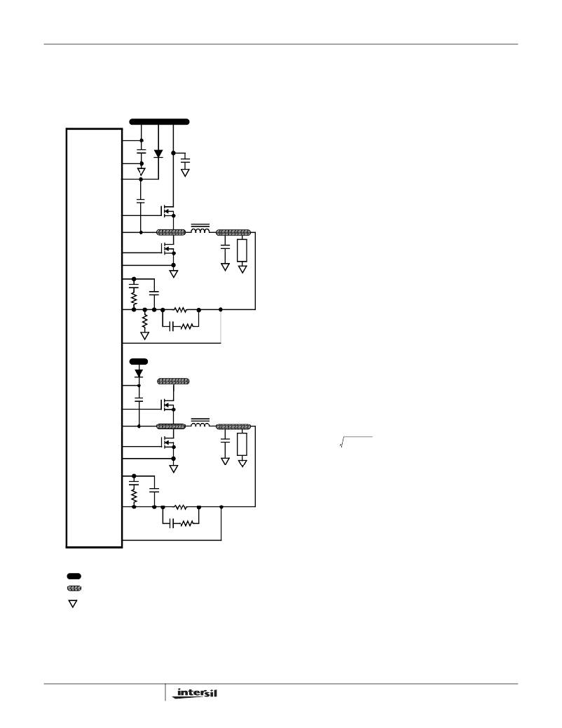 �
�
�ISL6530�
�nodes.� Use� copper� filled� polygons� on� the� top� and� bottom�
�circuit� layers� for� the� phase� nodes.� Use� the� remaining� printed�
�circuit� layers� for� small� signal� wiring.� The� wiring� traces� from�
�the� GATE� pins� to� the� MOSFET� gates� should� be� kept� short�
�and� wide� enough� to� easily� handle� the� 1A� of� drive� current.�
�+5V� V� IN�
�ISL6530�
�VCC�
�The� switching� components� should� be� placed� close� to� the�
�ISL6530� first.� Minimize� the� length� of� the� connections�
�between� the� input� capacitors,� C� IN� ,� and� the� power� switches�
�by� placing� them� nearby.� Position� both� the� ceramic� and� bulk�
�input� capacitors� as� close� to� the� upper� MOSFET� drain� as�
�possible.� Position� the� output� inductor� and� output� capacitors�
�between� the� upper� MOSFET� and� lower� diode� and� the� load.�
�The� critical� small� signal� components� include� any� bypass�
�GND�
�C� BP�
�D1�
�C� IN�
�capacitors,� feedback� components,� and� compensation�
�components.� Position� the� bypass� capacitor,� C� BP� ,� close� to� the�
�BOOT1�
�C� BOOT1�
�Q1�
�VCC� pin� with� a� via� directly� to� the� ground� plane.� Place� the�
�PWM� converter� compensation� components� close� to� the� FB�
�and� COMP� pins.� The� feedback� resistors� for� both� regulators�
�should� also� be� located� as� close� as� possible� to� the� relevant�
�UGATE1�
�PHASE1�
�L� OUT1�
�V� DDQ�
�FB� pin� with� vias� tied� straight� to� the� ground� plane� as� required.�
�PHASE1�
�Feedback� Compensation�
�LGATE1�
�PGND1�
�Q2�
�C� OUT1�
�Figure� 8� highlights� the� voltage-mode� control� loop� for� a�
�synchronous-rectified� buck� converter.� The� output� voltage�
�(V� OUT� )� is� regulated� to� the� Reference� voltage� level.� The�
�COMP1�
�FB1�
�C� 2A�
�R� 2A�
�R4�
�C� 1A�
�R� 1A�
�C� 3A� R� 3A�
�error� amplifier� (Error� Amp)� output� (V� E/A� )� is� compared� with�
�the� oscillator� (OSC)� triangular� wave� to� provide� a� pulse-�
�width� modulated� (PWM)� wave� with� an� amplitude� of� V� IN� at�
�the� PHASE� node.� The� PWM� wave� is� smoothed� by� the� output�
�filter� (L� O� and� C� O� ).�
�SENSE1�
�+5V� V� IN�
�The� modulator� transfer� function� is� the� small-signal� transfer�
�function� of� V� OUT� /V� E/A� .� This� function� is� dominated� by� a� DC�
�D2�
�V� DDQ�
�Gain� and� the� output� filter� (L� O� and� C� O� ),� with� a� double� pole�
�break� frequency� at� F� LC� and� a� zero� at� F� ESR� .� The� DC� Gain� of�
�BOOT2�
�C� BOOT2�
�Q3�
�the� modulator� is� simply� the� input� voltage� (V� IN� )� divided� by� the�
�peak-to-peak� oscillator� voltage� ?� V� OSC�
�UGATE2�
�PHASE2�
�L� OUT2�
�V� TT�
�Modulator� Break� Frequency� Equations�
�F� LC� =� ------------------------------------------�
�F� ESR� =� -------------------------------------------�
�PHASE2�
�LGATE2�
�Q4�
�C� OUT2�
�1�
�2� π� x� L� O� x� C� O�
�1�
�2� π� x� ESR� x� C� O�
�PGND2�
�COMP1�
�The� compensation� network� consists� of� the� error� amplifier�
�(internal� to� the� ISL6530)� and� the� impedance� networks� Z� IN�
�FB1�
�C� 2B�
�R� 2B�
�C� 1B�
�R� 1B�
�and� Z� FB� .� The� goal� of� the� compensation� network� is� to� provide�
�a� closed� loop� transfer� function� with� the� highest� 0dB� crossing�
�frequency� (f� 0dB� )� and� adequate� phase� margin.� Phase� margin�
�C� 3B� R� 3B�
�SENSE2�
�KEY�
�ISLAND� ON� POWER� PLANE� LAYER�
�ISLAND� ON� CIRCUIT� PLANE� LAYER�
�VIA� CONNECTION� TO� GROUND� PLANE�
�FIGURE� 7.� PRINTED� CIRCUIT� BOARD� POWER� PLANES�
�AND� ISLANDS�
�11�
�is� the� difference� between� the� closed� loop� phase� at� f� 0dB� and�
�180� degrees.� The� equations� below� relate� the� compensation�
�network’s� poles,� zeros� and� gain� to� the� components� (R� 1� ,� R� 2� ,�
�R� 3� ,� C� 1� ,� C� 2� ,� and� C� 3� )� in� Figure� 7.� Use� these� guidelines� for�
�locating� the� poles� and� zeros� of� the� compensation� network:�
�1.� Pick� gain� (R� 2� /R� 1� )� for� desired� converter� bandwidth.�
�2.� Place� first� zero� below� filter’s� double� pole� (~75%� F� LC� ).�
�3.� Place� second� zero� at� filter’s� double� pole.�
�4.� Place� first� pole� at� the� ESR� zero.�
�5.� Place� second� pole� at� half� the� switching� frequency.�
�6.� Check� gain� against� error� amplifier’s� open-loop� gain.�
�7.� Estimate� phase� margin� -� repeat� if� necessary.�
�FN9052.2�
�November� 15,� 2004�
�相关PDF资料 |
PDF描述 |
|---|---|
| ISL6531CRZ-T | IC CONTROLLER INTEL 32QFN |
| ISL6532AIRZ | IC REG/CTRLR ACPI DUAL DDR 28QFN |
| ISL6532BCRZ | IC REG/CTRLR ACPI DUAL DDR 20QFN |
| ISL6532CCRZ | IC REG/CTRLR ACPI DUAL DDR 28QFN |
| ISL6535CRZ | IC REG CTRLR BUCK PWM VM 16QFN |
相关代理商/技术参数 |
参数描述 |
|---|---|
| ISL6530CRZ | 功能描述:IC CONTROLLER INTEL 32QFN RoHS:是 类别:集成电路 (IC) >> PMIC - 稳压器 - 专用型 系列:- 标准包装:43 系列:- 应用:控制器,Intel VR11 输入电压:5 V ~ 12 V 输出数:1 输出电压:0.5 V ~ 1.6 V 工作温度:-40°C ~ 85°C 安装类型:表面贴装 封装/外壳:48-VFQFN 裸露焊盘 供应商设备封装:48-QFN(7x7) 包装:管件 |
| ISL6530CRZ-T | 功能描述:IC CONTROLLER INTEL 32QFN RoHS:是 类别:集成电路 (IC) >> PMIC - 稳压器 - 专用型 系列:- 标准包装:43 系列:- 应用:控制器,Intel VR11 输入电压:5 V ~ 12 V 输出数:1 输出电压:0.5 V ~ 1.6 V 工作温度:-40°C ~ 85°C 安装类型:表面贴装 封装/外壳:48-VFQFN 裸露焊盘 供应商设备封装:48-QFN(7x7) 包装:管件 |
| ISL6530EVAL1 | 功能描述:EVALUATION BOARD 1 ISL6530 RoHS:否 类别:编程器,开发系统 >> 评估板 - DC/DC 与 AC/DC(离线)SMPS 系列:- 产品培训模块:Obsolescence Mitigation Program 标准包装:1 系列:True Shutdown™ 主要目的:DC/DC,步升 输出及类型:1,非隔离 功率 - 输出:- 输出电压:- 电流 - 输出:1A 输入电压:2.5 V ~ 5.5 V 稳压器拓扑结构:升压 频率 - 开关:3MHz 板类型:完全填充 已供物品:板 已用 IC / 零件:MAX8969 |
| ISL6530EVAL2 | 功能描述:EVALUATION BOARD 2 ISL6530 RoHS:否 类别:编程器,开发系统 >> 评估板 - DC/DC 与 AC/DC(离线)SMPS 系列:- 产品培训模块:Obsolescence Mitigation Program 标准包装:1 系列:True Shutdown™ 主要目的:DC/DC,步升 输出及类型:1,非隔离 功率 - 输出:- 输出电压:- 电流 - 输出:1A 输入电压:2.5 V ~ 5.5 V 稳压器拓扑结构:升压 频率 - 开关:3MHz 板类型:完全填充 已供物品:板 已用 IC / 零件:MAX8969 |
| ISL6531CB | 功能描述:电压模式 PWM 控制器 Synch Buck - DDRAM RoHS:否 制造商:Texas Instruments 输出端数量:1 拓扑结构:Buck 输出电压:34 V 输出电流: 开关频率: 工作电源电压:4.5 V to 5.5 V 电源电流:600 uA 最大工作温度:+ 125 C 最小工作温度:- 40 C 封装 / 箱体:WSON-8 封装:Reel |
发布紧急采购,3分钟左右您将得到回复。