- 您现在的位置:买卖IC网 > PDF目录16597 > ISL6537ACR (Intersil)IC REG/CTRLR ACPI DUAL DDR 28QFN PDF资料下载
参数资料
| 型号: | ISL6537ACR |
| 厂商: | Intersil |
| 文件页数: | 13/16页 |
| 文件大小: | 0K |
| 描述: | IC REG/CTRLR ACPI DUAL DDR 28QFN |
| 标准包装: | 50 |
| 应用: | 存储器,DDR/DDR2 稳压器 |
| 电流 - 电源: | 7mA |
| 工作温度: | 0°C ~ 70°C |
| 安装类型: | 表面贴装 |
| 封装/外壳: | 28-VQFN 裸露焊盘 |
| 供应商设备封装: | 28-QFN(6x6) |
| 包装: | 管件 |
�� �
�
�ISL6537A�
�The� modulator� transfer� function� is� the� small-signal� transfer�
�function� of� V� OUT� /V� E/A� .� This� function� is� dominated� by� a� DC�
�100�
�F� Z1� F� Z2�
�F� P1�
�F� P2�
�Gain� and� the� output� filter� (L� O� and� C� O� ),� with� a� double� pole�
�80�
�break� frequency� at� F� LC� and� a� zero� at� F� ESR� .� The� DC� Gain� of�
�the� modulator� is� simply� the� input� voltage� (V� IN� )� divided� by� the�
�peak-to-peak� oscillator� voltage� Δ� V� OSC� .�
�Modulator� Break� Frequency� Equations�
�60�
�40�
�20�
�20LOG�
�(R� 2� /R� 1� )�
�OPEN� LOOP�
�ERROR� AMP� GAIN�
�20LOG�
�F� LC� =� -------------------------------------------�
�F� ESR� =� --------------------------------------------� (EQ.� 4)�
�F� LC�
�1� 1�
�2� π� x� LO� x� CO� 2� π� x� ESR� x� C� O�
�The� compensation� network� consists� of� the� error� amplifier�
�(internal� to� the� ISL6537A)� and� the� impedance� networks� Z� IN�
�and� Z� FB� .� The� goal� of� the� compensation� network� is� to� provide�
�a� closed� loop� transfer� function� with� the� highest� 0dB� crossing�
�frequency� (f� 0dB� )� and� adequate� phase� margin.� Phase� margin�
�0�
�-20�
�-40�
�-60�
�10�
�MODULATOR�
�GAIN�
�100�
�1K�
�(V� IN� /� Δ� V� OSC� )�
�F� ESR�
�10K� 100K� 1M�
�FREQUENCY� (Hz)�
�COMPENSATION�
�GAIN�
�CLOSED� LOOP�
�GAIN�
�10M�
�is� the� difference� between� the� closed� loop� phase� at� f� 0dB� and�
�180� degrees.� The� equations� below� relate� the� compensation�
�network’s� poles,� zeros� and� gain� to� the� components� (R� 1� ,� R� 2� ,�
�R� 3� ,� C� 1� ,� C� 2� ,� and� C� 3� )� in� Figure� 3.� Use� these� guidelines� for�
�locating� the� poles� and� zeros� of� the� compensation� network:�
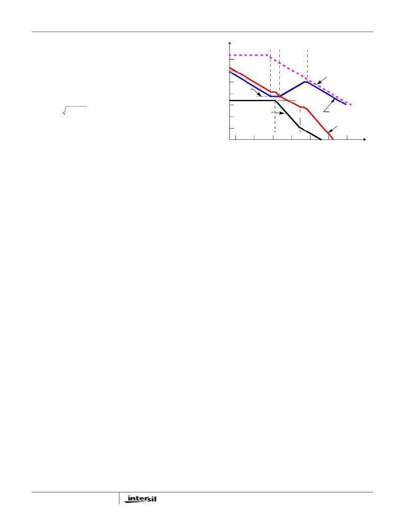
�FIGURE� 4.� ASYMPTOTIC� BODE� PLOT� OF� CONVERTER� GAIN�
�Output� Voltage� Selection�
�The� output� voltage� of� all� the� external� voltage� regulators� can�
�1.�
�2.�
�3.�
�4.�
�5.�
�6.�
�7.�
�Pick� Gain� (R� 2� /R� 1� )� for� desired� converter� bandwidth.�
�Place� 1� ST� Zero� Below� Filter’s� Double� Pole� (~75%� F� LC� ).�
�Place� 2� ND� Zero� at� Filter� ’s� Double� Pole.�
�Place� 1� ST� Pole� at� the� ESR� Zero.�
�Place� 2� ND� Pole� at� Half� the� Switching� Frequency.�
�Check� Gain� against� Error� Amplifier� ’s� Open-Loop� Gain.�
�Estimate� Phase� Margin� -� Repeat� if� Necessary.�
�be� programmed� to� any� level� between� their� individual� input�
�voltage� and� the� internal� reference,� 0.8V.� An� external� resistor�
�divider� is� used� to� scale� the� output� voltage� relative� to� the�
�reference� voltage� and� feed� it� back� to� the� inverting� input� of� the�
�error� amplifier,� refer� to� the� Typical� Application� on� page� 4.�
�The� output� voltage� programming� resistor� will� depend� on� the�
�value� chosen� for� the� feedback� resistor� and� the� desired�
�Compensation� Break� Frequency� Equations�
�output� voltage� of� the� particular� regulator.�
�F� Z1� =� ------------------------------------�
�F� P1� =� ---------------------------------------------------------�
�2� π� x� R� 2� x� ?� ----------------------� ?�
�R1� � 0.8V�
�1�
�2� π� x� R� 2� x� C� 1�
�1�
�?� C� 1� x� C� 2� ?�
�?� C� 1� +� C� 2� ?�
�R4� =� -----------------------------------�
�V� DDQ� –� 0.8V�
�F� Z2� =� -------------------------------------------------------�
�F� P2� =� ------------------------------------�
�R5� � 0.8V�
�1�
�2� π� x� (� R� 1� +� R� 3� )� x� C� 3�
�1�
�2� π� x� R� 3� x� C� 3�
�(EQ.� 5)�
�R8� =� ----------------------------------------�
�V� GMCH� –� 0.8V�
�R9� � 0.8V�
�R11� � 0.8V�
�Figure� 4� shows� an� asymptotic� plot� of� the� DC/DC� converter’s�
�gain� vs.� frequency.� The� actual� Modulator� Gain� has� a� high� gain�
�peak� due� to� the� high� Q� factor� of� the� output� filter� and� is� not�
�shown� in� Figure� 4.� Using� the� above� guidelines� should� give� a�
�Compensation� Gain� similar� to� the� curve� plotted.� The� open�
�loop� error� amplifier� gain� bounds� the� compensation� gain.�
�Check� the� compensation� gain� at� F� P2� with� the� capabilities� of�
�R10� =� -----------------------------------------------------------�
�xxxxxxxxxxxx�
�V� TT_GMCH/CPU� –� 0.8V�
�R12� =� ----------------------------------�
�V� DAC� –� 0.8V�
�(EQ.� 6)�
�the� error� amplifier.� The� Closed� Loop� Gain� is� constructed� on�
�the� graph� of� Figure� 4� by� adding� the� Modulator� Gain� (in� dB)� to�
�the� Compensation� Gain� (in� dB).� This� is� equivalent� to�
�multiplying� the� modulator� transfer� function� to� the�
�compensation� transfer� function� and� plotting� the� gain.�
�The� compensation� gain� uses� external� impedance� networks�
�Z� FB� and� Z� IN� to� provide� a� stable,� high� bandwidth� (BW)� overall�
�loop.� A� stable� control� loop� has� a� gain� crossing� with�
�-20dB/decade� slope� and� a� phase� margin� greater� than� 45�
�degrees.� Include� worst� case� component� variations� when�
�determining� phase� margin.�
�13�
�If� the� output� voltage� desired� is� 0.8V,� simply� route� the� output�
�voltage� back� to� the� respective� FB� pin� through� the� feedback�
�resistor� and� do� not� populate� the� output� voltage� programming�
�resistor.�
�The� output� voltage� for� the� internal� V� TT_DDR� linear� regulator�
�is� set� internal� to� the� ISL6537A� to� track� the� V� DDQ� voltage� by�
�50%.� There� is� no� need� for� external� programming� resistors.�
�FN9143.5�
�相关PDF资料 |
PDF描述 |
|---|---|
| M3AAA-3036J | IDC CABLE - MSC30A/MC34G/MSC30A |
| GBC18DRES-S93 | CONN EDGECARD 36POS .100 EYELET |
| RBC22DRTI-S13 | CONN EDGECARD 44POS .100 EXTEND |
| GEC28DREN-S93 | CONN EDGECARD 56POS .100 EYELET |
| GEC28DREH-S93 | CONN EDGECARD 56POS .100 EYELET |
相关代理商/技术参数 |
参数描述 |
|---|---|
| ISL6537ACRR5160 | 制造商:Intersil Corporation 功能描述: |
| ISL6537ACR-T | 功能描述:IC REG/CTRLR ACPI DUAL DDR 28QFN RoHS:否 类别:集成电路 (IC) >> PMIC - 电源管理 - 专用 系列:- 应用说明:Ultrasound Imaging Systems Application Note 产品培训模块:Lead (SnPb) Finish for COTS Obsolescence Mitigation Program 标准包装:37 系列:- 应用:医疗用超声波成像,声纳 电流 - 电源:- 电源电压:2.37 V ~ 6 V 工作温度:0°C ~ 70°C 安装类型:表面贴装 封装/外壳:56-WFQFN 裸露焊盘 供应商设备封装:56-TQFN-EP(8x8) 包装:管件 |
| ISL6537ACRZ | 功能描述:IC REG/CTRLR ACPI DUAL DDR 28QFN RoHS:是 类别:集成电路 (IC) >> PMIC - 电源管理 - 专用 系列:- 应用说明:Ultrasound Imaging Systems Application Note 产品培训模块:Lead (SnPb) Finish for COTS Obsolescence Mitigation Program 标准包装:37 系列:- 应用:医疗用超声波成像,声纳 电流 - 电源:- 电源电压:2.37 V ~ 6 V 工作温度:0°C ~ 70°C 安装类型:表面贴装 封装/外壳:56-WFQFN 裸露焊盘 供应商设备封装:56-TQFN-EP(8x8) 包装:管件 |
| ISL6537ACRZR5160 | 功能描述:IC REG/CTRLR ACPI DUAL DDR 28QFN RoHS:是 类别:集成电路 (IC) >> PMIC - 电源管理 - 专用 系列:- 应用说明:Ultrasound Imaging Systems Application Note 产品培训模块:Lead (SnPb) Finish for COTS Obsolescence Mitigation Program 标准包装:37 系列:- 应用:医疗用超声波成像,声纳 电流 - 电源:- 电源电压:2.37 V ~ 6 V 工作温度:0°C ~ 70°C 安装类型:表面贴装 封装/外壳:56-WFQFN 裸露焊盘 供应商设备封装:56-TQFN-EP(8x8) 包装:管件 |
| ISL6537ACRZ-T | 功能描述:IC REG/CTLR ACPI DUAL DDR 28QFN RoHS:是 类别:集成电路 (IC) >> PMIC - 电源管理 - 专用 系列:- 产品培训模块:Lead (SnPb) Finish for COTS Obsolescence Mitigation Program 标准包装:50 系列:- 应用:热电冷却器 电流 - 电源:- 电源电压:3 V ~ 5.5 V 工作温度:-40°C ~ 85°C 安装类型:表面贴装 封装/外壳:28-SOIC(0.173",4.40mm 宽)裸露焊盘 供应商设备封装:28-TSSOP 裸露焊盘 包装:管件 产品目录页面:1410 (CN2011-ZH PDF) |
发布紧急采购,3分钟左右您将得到回复。