参数资料
| 型号: | ISL6554CB-T |
| 厂商: | Intersil |
| 文件页数: | 12/16页 |
| 文件大小: | 0K |
| 描述: | IC PWM CORE VOLTAGE REG 20-SOIC |
| 标准包装: | 1,000 |
| 应用: | 控制器,Intel Itanium? |
| 输入电压: | 4.75 V ~ 5.25 V |
| 输出数: | 4 |
| 输出电压: | 0.95 V ~ 1.7 V |
| 工作温度: | 0°C ~ 70°C |
| 安装类型: | 表面贴装 |
| 封装/外壳: | 20-SOIC(0.295",7.50mm 宽) |
| 供应商设备封装: | 20-SOIC W |
| 包装: | 带卷 (TR) |
�� �
�
�ISL6554�
�resistor� R� T� .� To� avoid� pickup� by� the� FS/DIS� pin,� it� is� important�
�to� place� this� resistor� next� to� the� pin.�
�25�
�20�
�15�
�10�
�5�
�0�
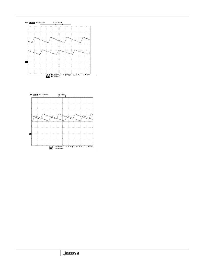
�FIGURE� 8.� TWO� CHANNEL� MULTI-PHASE� SYSTEM� WITH�
�CURRENT� BALANCING� DISABLED�
�25�
�Layout� Considerations�
�MOSFETs� switch� very� fast� and� efficiently.� The� speed� with�
�which� the� current� transitions� from� one� device� to� another�
�causes� voltage� spikes� across� the� interconnecting� impedances�
�and� parasitic� circuit� elements.� These� voltage� spikes� can�
�degrade� efficiency,� radiate� noise� into� the� circuit� and� lead� to�
�device� overvoltage� stress.� Careful� component� layout� and�
�printed� circuit� design� minimizes� the� voltage� spikes� in� the�
�converter.� Consider,� as� an� example,� the� turnoff� transition� of�
�the� upper� PWM� MOSFET.� Prior� to� turnoff,� the� upper� MOSFET�
�was� carrying� channel� current.� During� the� turnoff,� current� stops�
�flowing� in� the� upper� MOSFET� and� is� picked� up� by� the� lower�
�MOSFET.� Any� inductance� in� the� switched� current� path�
�generates� a� large� voltage� spike� during� the� switching� interval.�
�Careful� component� selection,� tight� layout� of� the� critical�
�components,� and� short,� wide� circuit� traces� minimize� the�
�magnitude� of� voltage� spikes.� Contact� Intersil� for� evaluation�
�board� drawings� of� the� component� placement� and� printed�
�circuit� board.�
�20�
�where� I� LT�
�Then:� R� ISEN�
�15�
�10�
�5�
�0�
�FIGURE� 9.� TWO� CHANNEL� MULTI-PHASE� SYSTEM� WITH�
�CURRENT� BALANCING� ENABLED�
�As� discussed� previously,� the� voltage� drop� across� each� Q2�
�transistor� at� the� point� in� time� when� current� is� sampled� is� r� DSON�
�(Q2)� x� I� SAMPLE� .� The� voltage� at� Q2’s� drain,� the� PHASE� node,�
�is� applied� through� the� R� ISEN� resistor� to� the� ISL6554� ISEN� pin.�
�This� pin� is� held� at� virtual� ground,� so� the� current� into� ISEN� is:�
�I� SENSE� =� I� SAMPLE� x� r� DS(ON)� (Q2)� /� R� ISEN� .�
�R� Isen� =� I� SAMPLE� x� r� DS(ON)� (Q2)� /� 50� μ� A�
�Example:� From� the� previous� conditions,�
�=� 100A,�
�I� SAMPLE� =� 25.49A,�
�r� DS(ON)� (Q2)� =� 4m� ?�
�=� 2.04K� and�
�I� CURRENT� TRIP� =� 165%�
�There� are� two� sets� of� critical� components� in� a� DC-DC�
�converter� using� a� ISL6554� controller� and� a� HIP6601� gate�
�driver.� The� power� components� are� the� most� critical� because�
�they� switch� large� amounts� of� energy.� Next� are� small� signal�
�components� that� connect� to� sensitive� nodes� or� supply� critical�
�bypassing� current� and� signal� coupling.�
�The� power� components� should� be� placed� first.� Locate� the�
�input� capacitors� close� to� the� power� switches.� Minimize� the�
�length� of� the� connections� between� the� input� capacitors,� C� IN� ,�
�and� the� power� switches.� Locate� the� output� inductors� and�
�output� capacitors� between� the� MOSFETs� and� the� load.�
�Locate� the� gate� driver� close� to� the� MOSFETs.�
�The� critical� small� components� include� the� bypass� capacitors� for�
�VCC� and� PVCC� on� the� gate� driver� ICs.� Locate� the� bypass�
�capacitor,� C� BP� ,� for� the� ISL6554� controller� close� to� the� device.� It�
�is� especially� important� to� locate� the� resistors� associated� with�
�the� input� to� the� amplifiers� close� to� their� respective� pins,� since�
�they� represent� the� input� to� feedback� amplifiers.� Resistor� R� T� ,�
�that� sets� the� oscillator� frequency� should� also� be� located� next� to�
�the� associated� pin.� It� is� especially� important� to� place� the� R� SEN�
�resistors� at� the� respective� terminals� of� the� ISL6554.�
�A� multi-layer� printed� circuit� board� is� recommended.� Figure� 11�
�shows� the� connections� of� the� critical� components� for� one�
�output� channel� of� the� converter.� Note� that� capacitors� C� IN� and�
�C� OUT� could� each� represent� numerous� physical� capacitors.�
�Dedicate� one� solid� layer,� usually� the� middle� layer� of� the� PC�
�Short� circuit� I� LT�
�=� 165A.�
�board,� for� a� ground� plane� and� make� all� critical� component�
�Channel� Frequency� Oscillator�
�The� channel� oscillator� frequency� is� set� by� placing� a� resistor,�
�R� T� ,� to� ground� from� the� FS/DIS� pin.� Figure� 10� is� a� curve�
�showing� the� relationship� between� frequency,� F� SW� ,� and�
�12�
�ground� connections� with� vias� to� this� layer.� Dedicate� another�
�solid� layer� as� a� power� plane� and� break� this� plane� into� smaller�
�islands� of� common� voltage� levels.� Keep� the� metal� runs� from�
�the� PHASE� terminal� to� output� inductor� short.� The� power� plane�
�should� support� the� input� power� and� output� power� nodes.� Use�
�FN9003.3�
�February� 11,� 2005�
�相关PDF资料 |
PDF描述 |
|---|---|
| ISL6556ACR-T | IC CTRLR MULTIPHASE VRM10 32-QFN |
| ISL6556BCR-T | IC CTRLR MULTIPHASE VRM10 32-QFN |
| ISL6557ACB-T | IC REG CTRLR BUCK PWM VM 24-SOIC |
| ISL6558IR-T | IC REG CTRLR BUCK PWM 20-QFN |
| ISL6559CBZ-T | IC REG CTRLR BUCK PWM VM 28-SOIC |
相关代理商/技术参数 |
参数描述 |
|---|---|
| ISL6554CB-TR5165 | 制造商:Rochester Electronics LLC 功能描述: 制造商:Intersil Corporation 功能描述: |
| ISL6554CBZ | 功能描述:IC PWM CORE VOLTAGE REG 20-SOIC RoHS:是 类别:集成电路 (IC) >> PMIC - 稳压器 - 专用型 系列:- 产品培训模块:Lead (SnPb) Finish for COTS Obsolescence Mitigation Program 标准包装:2,000 系列:- 应用:电源,ICERA E400,E450 输入电压:4.1 V ~ 5.5 V 输出数:10 输出电压:可编程 工作温度:-40°C ~ 85°C 安装类型:表面贴装 封装/外壳:42-WFBGA,WLCSP 供应商设备封装:42-WLP 包装:带卷 (TR) |
| ISL6554CBZA | 功能描述:IC PWM CORE VOLTAGE REG 20-SOIC RoHS:是 类别:集成电路 (IC) >> PMIC - 稳压器 - 专用型 系列:- 产品培训模块:Lead (SnPb) Finish for COTS Obsolescence Mitigation Program 标准包装:2,000 系列:- 应用:电源,ICERA E400,E450 输入电压:4.1 V ~ 5.5 V 输出数:10 输出电压:可编程 工作温度:-40°C ~ 85°C 安装类型:表面贴装 封装/外壳:42-WFBGA,WLCSP 供应商设备封装:42-WLP 包装:带卷 (TR) |
| ISL6554CBZA-T | 功能描述:IC PWM CORE VOLTAGE REG 20-SOIC RoHS:是 类别:集成电路 (IC) >> PMIC - 稳压器 - 专用型 系列:- 产品培训模块:Lead (SnPb) Finish for COTS Obsolescence Mitigation Program 标准包装:2,000 系列:- 应用:电源,ICERA E400,E450 输入电压:4.1 V ~ 5.5 V 输出数:10 输出电压:可编程 工作温度:-40°C ~ 85°C 安装类型:表面贴装 封装/外壳:42-WFBGA,WLCSP 供应商设备封装:42-WLP 包装:带卷 (TR) |
| ISL6554CBZ-T | 功能描述:IC PWM CORE VOLTAGE REG 20-SOIC RoHS:是 类别:集成电路 (IC) >> PMIC - 稳压器 - 专用型 系列:- 产品培训模块:Lead (SnPb) Finish for COTS Obsolescence Mitigation Program 标准包装:2,000 系列:- 应用:电源,ICERA E400,E450 输入电压:4.1 V ~ 5.5 V 输出数:10 输出电压:可编程 工作温度:-40°C ~ 85°C 安装类型:表面贴装 封装/外壳:42-WFBGA,WLCSP 供应商设备封装:42-WLP 包装:带卷 (TR) |
发布紧急采购,3分钟左右您将得到回复。