参数资料
| 型号: | ISL6556BCRZ-T |
| 厂商: | Intersil |
| 文件页数: | 11/24页 |
| 文件大小: | 0K |
| 描述: | IC CTRLR MULTIPHASE VRM10 32-QFN |
| 标准包装: | 6,000 |
| 应用: | 控制器,Intel VR10X |
| 输入电压: | 3 V ~ 12 V |
| 输出数: | 4 |
| 输出电压: | 0.84 V ~ 1.6 V |
| 工作温度: | 0°C ~ 70°C |
| 安装类型: | 表面贴装 |
| 封装/外壳: | 32-VFQFN 裸露焊盘 |
| 供应商设备封装: | 32-QFN 裸露焊盘(5x5) |
| 包装: | 带卷 (TR) |
�� �
�
�ISL6556B�
�Figures� 14,� 16� and� 16� in� the� section� entitled� Input� Capacitor�
�Selection� can� be� used� to� determine� the� input-capacitor� RMS�
�current� based� on� load� current,� duty� cycle,� and� the� number� of�
�channels.� They� are� provided� as� aids� in� determining� the�
�switching� cycle.� The� sampled� current,� I� n� ,� is� used� for� channel-�
�current� balance,� load-line� regulation,� overcurrent� protection,�
�and� module� current� sharing.� From� Figure� 3,� the� following�
�equation� for� I� n� is� derived�
�I� n� =� I� L� ----------------------� )�
�optimal� input� capacitor� solution.� Figure� 17� shows� the� single�
�phase� input-capacitor� RMS� current� for� comparison.�
�r� DS� (� ON�
�R� ISEN�
�(EQ.� 3)�
�PWM� Operation�
�The� timing� of� each� converter� leg� is� set� by� the� number� of�
�active� channels.� The� default� channel� setting� for� the�
�ISL6556B� is� four.� One� switching� cycle� is� defined� as� the� time�
�between� PWM1� pulse� termination� signals.� The� pulse�
�termination� signal� is� the� internally� generated� clock� signal�
�that� triggers� the� falling� edge� of� PWM1.� The� cycle� time� of� the�
�pulse� termination� signal� is� the� inverse� of� the� switching�
�frequency� set� by� the� resistor� between� the� FS� pin� and�
�ground.� Each� cycle� begins� when� the� clock� signal� commands�
�where� I� L� is� the� channel� current.�
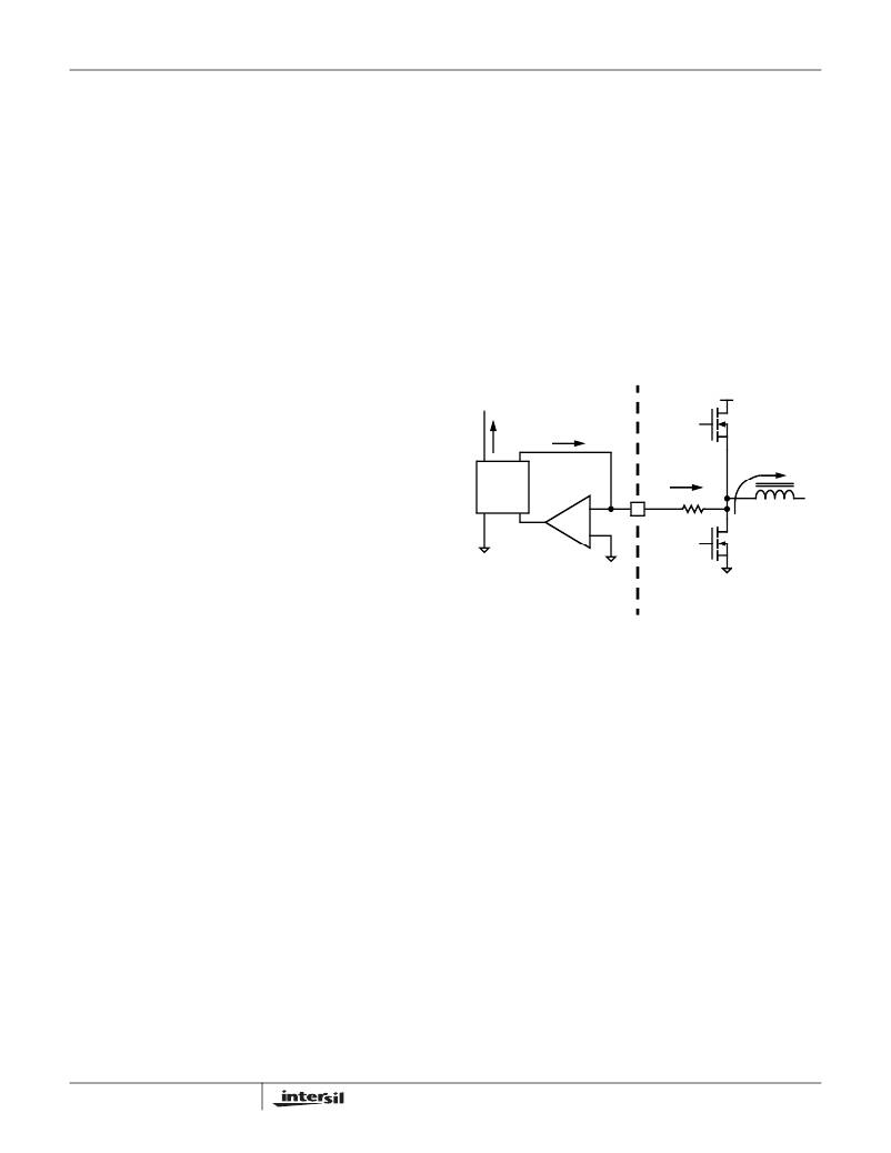
�If� R� DS(ON)� sensing� is� not� desired,� an� independent� current-�
�sense� resistor� in� series� with� the� lower� MOSFET� source� can�
�serve� as� a� sense� element.� The� circuitry� shown� in� Figure� 3�
�represents� channel� n� of� an� N-channel� converter.� This�
�circuitry� is� repeated� for� each� channel� in� the� converter,� but�
�may� not� be� active� depending� upon� the� status� of� the� PWM3�
�and� PWM4� pins� as� described� under� PWM� Operation�
�section.�
�I� SEN� =� I� -------------------------� )� -�
�L� R�
�the� channel-1� PWM� output� to� go� low.� The� PWM1� transition�
�signals� the� channel-1� MOSFET� driver� to� turn� off� the�
�channel-1� upper� MOSFET� and� turn� on� the� channel-1�
�synchronous� MOSFET.� In� the� default� channel� configuration,�
�I� n�
�r� DS� (� ON�
�ISEN�
�V� IN�
�CHANNEL� N�
�UPPER� MOSFET�
�the� PWM2� pulse� terminates� 1/4� of� a� cycle� after� PWM1.� The�
�PWM3� output� follows� another� 1/4� of� a� cycle� after� PWM2.�
�PWM4� terminates� another� 1/4� of� a� cycle� after� PWM3.�
�SAMPLE�
�&�
�HOLD�
�ISEN(n)�
�I� L�
�If� PWM3� is� connected� to� VCC,� two� channel� operation� is�
�selected� and� the� PWM2� pulse� terminates� 1/2� of� a� cycle� later.�
�Connecting� PWM4� to� VCC� selects� three� channel� operation�
�and� the� pulse-termination� times� are� spaced� in� 1/3� cycle�
�-�
�+�
�R� ISEN�
�CHANNEL� N�
�-�
�+�
�I� L� r� DS� (� ON� )�
�increments.�
�LOWER� MOSFET�
�Once� a� PWM� signal� transitions� low,� it� is� held� low� for� a�
�ISL6556B� INTERNAL� CIRCUIT�
�EXTERNAL� CIRCUIT�
�I� 1� +� I� 2� +� +� I� N�
�I� AVG� =� ----------------------------------------�
�N�
�I� AVG� =� -------------� ----------------------� )�
�R� ISEN�
�minimum� of� 1/3� cycle.� This� forced� off� time� is� required� to�
�ensure� an� accurate� current� sample.� Current� sensing� is�
�described� in� the� next� section.� After� the� forced� off� time�
�expires,� the� PWM� output� is� enabled.� The� PWM� output� state�
�is� driven� by� the� position� of� the� error� amplifier� output� signal,�
�V� COMP� ,� minus� the� current� correction� signal� relative� to� the�
�sawtooth� ramp� as� illustrated� in� Figure� 4.� When� the� modified�
�V� COMP� voltage� crosses� the� sawtooth� ramp,� the� PWM� output�
�transitions� high.� The� MOSFET� driver� detects� the� change� in�
�state� of� the� PWM� signal� and� turns� off� the� synchronous�
�MOSFET� and� turns� on� the� upper� MOSFET.� The� PWM� signal�
�will� remain� high� until� the� pulse� termination� signal� marks� the�
�beginning� of� the� next� cycle� by� triggering� the� PWM� signal� low.�
�Current� Sensing�
�During� the� forced� off� time� following� a� PWM� transition� low,� the�
�controller� senses� channel� current� by� sampling� the� voltage�
�across� the� lower� MOSFET� r� DS(ON)� (see� Figure� 3).� A� ground-�
�referenced� operational� amplifier,� internal� to� the� ISL6556B,� is�
�connected� to� the� PHASE� node� through� a� resistor,� R� ISEN� .�
�The� voltage� across� R� ISEN� is� equivalent� to� the� voltage� drop�
�across� the� r� DS(ON)� of� the� lower� MOSFET� while� it� is�
�conducting.� The� resulting� current� into� the� ISEN� pin� is�
�proportional� to� the� channel� current,� I� L� .� The� ISEN� current� is�
�sampled� and� held� after� sufficient� settling� time� every�
�11�
�FIGURE� 3.� INTERNAL� AND� EXTERNAL� CURRENT-SENSING�
�CIRCUITRY�
�Channel-Current� Balance�
�The� sampled� current,� I� n� ,� from� each� active� channel� is� used� to�
�gauge� both� overall� load� current� and� the� relative� channel�
�current� carried� in� each� leg� of� the� converter.� The� individual�
�sample� currents� are� summed� and� divided� by� the� number� of�
�active� channels.� The� resulting� average� current,� I� AVG� ,�
�provides� a� measure� of� the� total� load� current� demand� on� the�
�converter� and� the� appropriate� level� of� channel� current.� Using�
�Figures� 3� and� 4,� the� average� current� is� defined� as�
�…�
�(EQ.� 4)�
�I� OUT� r� DS� (� ON�
�N�
�where� N� is� the� number� of� active� channels� and� I� OUT� is� the�
�total� load� current.�
�The� average� current� is� subtracted� from� the� individual�
�channel� sample� currents.� The� resulting� error� current,� I� ER� ,� is�
�filtered� to� modify� V� COMP� .� The� modified� V� COMP� signal� is�
�compared� to� a� sawtooth� ramp� signal� to� produce� a� modified�
�FN9097.4�
�December� 28,� 2004�
�相关PDF资料 |
PDF描述 |
|---|---|
| ESC35DRTI-S734 | CONN EDGECARD 70POS DIP .100 SLD |
| ISL6568CRZR5184 | IC CTRLR PWM 2PHASE BUCK 32-QFN |
| ISL6334ACRZR5368 | IC CTRLR PWM 4PHASE BUCK 40QFN |
| NCP4640H020T1G | IC REG LDO 2V 50MA SOT89-5 |
| ISL6334ACRZ-TR5368 | IC CTRLR PWM 4PHASE BUCK 40QFN |
相关代理商/技术参数 |
参数描述 |
|---|---|
| ISL6557 WAF | 制造商:Intersil Corporation 功能描述: |
| ISL6557ACB | 功能描述:IC REG CTRLR BUCK PWM VM 24-SOIC RoHS:否 类别:集成电路 (IC) >> PMIC - 稳压器 - DC DC 切换控制器 系列:- 标准包装:4,000 系列:- PWM 型:电压模式 输出数:1 频率 - 最大:1.5MHz 占空比:66.7% 电源电压:4.75 V ~ 5.25 V 降压:是 升压:无 回扫:无 反相:无 倍增器:无 除法器:无 Cuk:无 隔离:无 工作温度:-40°C ~ 85°C 封装/外壳:40-VFQFN 裸露焊盘 包装:带卷 (TR) |
| ISL6557ACB-T | 功能描述:IC REG CTRLR BUCK PWM VM 24-SOIC RoHS:否 类别:集成电路 (IC) >> PMIC - 稳压器 - DC DC 切换控制器 系列:- 标准包装:4,000 系列:- PWM 型:电压模式 输出数:1 频率 - 最大:1.5MHz 占空比:66.7% 电源电压:4.75 V ~ 5.25 V 降压:是 升压:无 回扫:无 反相:无 倍增器:无 除法器:无 Cuk:无 隔离:无 工作温度:-40°C ~ 85°C 封装/外壳:40-VFQFN 裸露焊盘 包装:带卷 (TR) |
| ISL6557ACBZ | 功能描述:IC REG CTRLR BUCK PWM VM 24-SOIC RoHS:是 类别:集成电路 (IC) >> PMIC - 稳压器 - DC DC 切换控制器 系列:- 产品培训模块:Lead (SnPb) Finish for COTS Obsolescence Mitigation Program 标准包装:2,500 系列:- PWM 型:电流模式 输出数:1 频率 - 最大:275kHz 占空比:50% 电源电压:18 V ~ 110 V 降压:无 升压:无 回扫:无 反相:无 倍增器:无 除法器:无 Cuk:无 隔离:是 工作温度:-40°C ~ 85°C 封装/外壳:8-SOIC(0.154",3.90mm 宽) 包装:带卷 (TR) |
| ISL6557ACBZ-T | 功能描述:IC REG CTRLR BUCK PWM VM 24-SOIC RoHS:是 类别:集成电路 (IC) >> PMIC - 稳压器 - DC DC 切换控制器 系列:- 产品培训模块:Lead (SnPb) Finish for COTS Obsolescence Mitigation Program 标准包装:2,500 系列:- PWM 型:电流模式 输出数:1 频率 - 最大:275kHz 占空比:50% 电源电压:18 V ~ 110 V 降压:无 升压:无 回扫:无 反相:无 倍增器:无 除法器:无 Cuk:无 隔离:是 工作温度:-40°C ~ 85°C 封装/外壳:8-SOIC(0.154",3.90mm 宽) 包装:带卷 (TR) |
发布紧急采购,3分钟左右您将得到回复。